- 您现在的位置:买卖IC网 > PDF目录17065 > EVAL-AD5760SDZ (Analog Devices Inc)BOARD EVAL FOR AD5760SDZ PDF资料下载
参数资料
| 型号: | EVAL-AD5760SDZ |
| 厂商: | Analog Devices Inc |
| 文件页数: | 27/28页 |
| 文件大小: | 0K |
| 描述: | BOARD EVAL FOR AD5760SDZ |
| 标准包装: | 1 |
| 系列: | * |
第1页第2页第3页第4页第5页第6页第7页第8页第9页第10页第11页第12页第13页第14页第15页第16页第17页第18页第19页第20页第21页第22页第23页第24页第25页第26页当前第27页第28页
AD5760
Data Sheet
Rev. D | Page 8 of 28
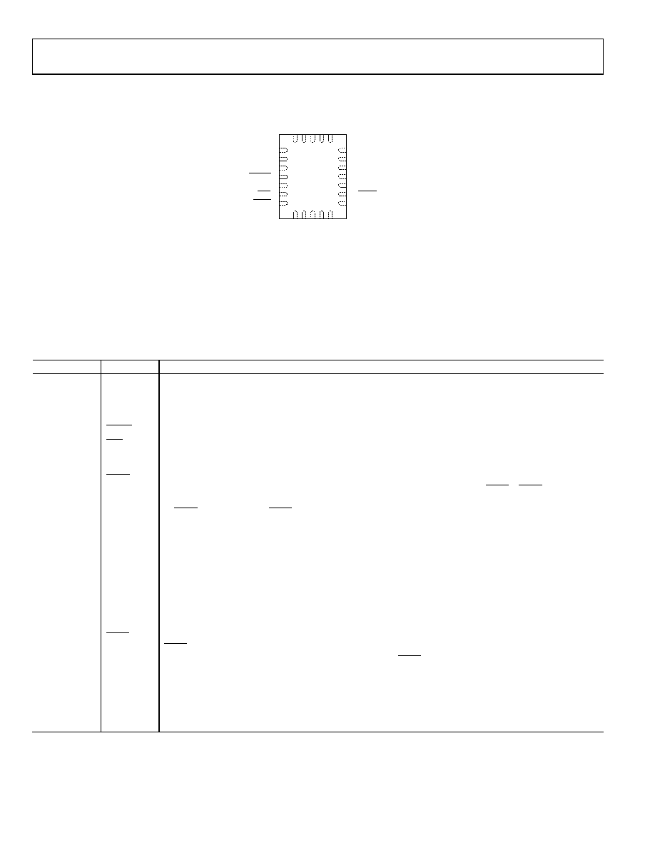
PIN CONFIGURATION AND FUNCTION DESCRIPTIONS
IN
V
IO
V
CC
V
CC
AGND
VSS
VREFN
SD
O
DNC
SD
IN
R
FB
AD5760
TOP VIEW
(Not to Scale)
VOUT
VREFP
RESET
VDD
CLR
LDAC
SYNC
DGND
SCLK
2
1
3
4
5
6
7
18
19
17
16
15
14
13
9
1
0
1
2
8
2
1
2
0
2
3
2
4
09
650
-00
5
NOTES
1. DNC = DO NOT CONNECT. DO NOT CONNECT TO THIS PIN.
2. NEGATIVE ANALOG SUPPLY CONNECTION (VSS).
A VOLTAGE IN THE RANGE OF –16.5 V TO –2.5 V
CAN BE CONNECTED. VSS SHOULD BE DECOUPLED
TO AGND. THE PADDLE CAN BE LEFT ELECTRICALLY
UNCONNECTED PROVIDED THAT A SUPPLY
CONNECTION IS MADE AT THE VSS PINS. IT IS
RECOMMENDED THAT THE PADDLE BE THERMALLY
CONNECTED TO A COPPER PLANE FOR ENHANCED
THERMAL PERFORMANCE.
Figure 4. Pin Configuration
Table 5. Pin Function Descriptions
Pin No.
Mnemonic
Description
1
VOUT
Analog Output Voltage.
2
VREFP
Positive Reference Voltage Input. A voltage in the range of 5 V to VDD 2.5 V can be connected to this pin.
3, 5
VDD
Positive Analog Supply Connection. A voltage in the range of 7.5 V to 16.5 V can be connected to this pin.
VDD must be decoupled to AGND.
4
RESET
Active Low Reset. Asserting this pin returns the AD5760 to its power-on status.
6
CLR
Active Low Input. Asserting this pin sets the DAC register to a user defined value (see Table 12) and updates
the DAC output. The output value depends on the DAC register coding that is being used, either binary or
twos complement.
7
LDAC
Active Low Load DAC Logic Input. This pin is used to update the DAC register and, consequently, the analog
output. When tied permanently low, the output is updated on the rising edge of SYNC. If LDAC is held high
during the write cycle, the input register is updated, but the output update is held off until the falling edge
of LDAC. Do not leave the LDAC pin unconnected.
8
VCC
Digital Supply. Voltage range is from 2.7 V to 5.5 V. VCC should be decoupled to DGND.
9
IOVCC
Digital Interface Supply. Digital threshold levels are referenced to the voltage applied to this pin. Voltage
range is from 1.71 V to 5.5 V.
10, 21, 22, 23
DNC
Do Not Connect. Do not connect to these pins.
11
SDO
Serial Data Output. Data is clocked out on the rising edge of the serial clock input.
12
SDIN
Serial Data Input. This device has a 24-bit input shift register. Data is clocked into the register on the falling
edge of the serial clock input.
13
SCLK
Serial Clock Input. Data is clocked into the input shift register on the falling edge of the serial clock input.
Data can be transferred at rates of up to 35 MHz.
14
SYNC
Level Triggered Control Input (Active Low). This is the frame synchronization signal for the input data. When
SYNC goes low, it enables the input shift register, and data is then transferred in on the falling edges of the
following clocks. The DAC is updated on the rising edge of SYNC.
15
DGND
Ground Reference Pin for Digital Circuitry.
16
VREFN
Negative Reference Voltage Input.
17, 18
VSS
Negative Analog Supply Connection. A voltage in the range of 16.5 V to 2.5 V can be connected to this
pin. VSS must be decoupled to AGND.
19
AGND
Ground Reference Pin for Analog Circuitry.
相关PDF资料 |
PDF描述 |
|---|---|
| HKQ0603S4N7C-T | INDUCTOR HI FREQ 4.7NH 0201 |
| LGU2D471MELZ | CAP ALUM 470UF 200V 20% SNAP |
| SEK331M100ST | CAP ALUM 330UF 100V 20% RADIAL |
| MC56F8006DEMO | DEMO BOARD FOR MC56F8006 |
| 380LX332M050J012 | CAP ALUM 3300UF 50V 20% SNAP |
相关代理商/技术参数 |
参数描述 |
|---|---|
| EVAL-AD5764EB | 制造商:Analog Devices 功能描述:EVALUATION BOARD FOR QUAD, 16-BIT, HIGH ACCURACY, SERIAL INPUT, BIPOLAR VOLTAGE OUTPUT DAC 制造商:Analog Devices 功能描述:EVALUATION CONTROL BOARD I.C. - Bulk |
| EVAL-AD5764EBZ | 功能描述:BOARD EVAL FOR AD5764 RoHS:是 类别:编程器,开发系统 >> 评估板 - 数模转换器 (DAC) 系列:- 产品培训模块:Lead (SnPb) Finish for COTS Obsolescence Mitigation Program 标准包装:1 系列:- DAC 的数量:4 位数:12 采样率(每秒):- 数据接口:串行,SPI? 设置时间:3µs DAC 型:电流/电压 工作温度:-40°C ~ 85°C 已供物品:板 已用 IC / 零件:MAX5581 |
| EVAL-AD5764REBZ | 功能描述:EVAL BOARD FOR AD5764 RoHS:是 类别:编程器,开发系统 >> 评估板 - 数模转换器 (DAC) 系列:- 产品培训模块:Lead (SnPb) Finish for COTS Obsolescence Mitigation Program 标准包装:1 系列:- DAC 的数量:4 位数:12 采样率(每秒):- 数据接口:串行,SPI? 设置时间:3µs DAC 型:电流/电压 工作温度:-40°C ~ 85°C 已供物品:板 已用 IC / 零件:MAX5581 |
| EVAL-AD5765EBZ | 功能描述:BOARD EVAL FOR AD5765 RoHS:是 类别:编程器,开发系统 >> 评估板 - 数模转换器 (DAC) 系列:* 产品培训模块:Lead (SnPb) Finish for COTS Obsolescence Mitigation Program 标准包装:1 系列:- DAC 的数量:4 位数:12 采样率(每秒):- 数据接口:串行,SPI? 设置时间:3µs DAC 型:电流/电压 工作温度:-40°C ~ 85°C 已供物品:板 已用 IC / 零件:MAX5581 |
| EVAL-AD5780SDZ | 功能描述:BOARD EVALUATION FOR AD5780 RoHS:是 类别:编程器,开发系统 >> 评估板 - 数模转换器 (DAC) 系列:- 产品培训模块:Lead (SnPb) Finish for COTS Obsolescence Mitigation Program 标准包装:1 系列:- DAC 的数量:4 位数:12 采样率(每秒):- 数据接口:串行,SPI? 设置时间:3µs DAC 型:电流/电压 工作温度:-40°C ~ 85°C 已供物品:板 已用 IC / 零件:MAX5581 |
发布紧急采购,3分钟左右您将得到回复。