- 您现在的位置:买卖IC网 > PDF目录16231 > EVAL-AD5934EBZ (Analog Devices Inc)BOARD EVALUATION FOR AD5934 PDF资料下载
参数资料
| 型号: | EVAL-AD5934EBZ |
| 厂商: | Analog Devices Inc |
| 文件页数: | 18/32页 |
| 文件大小: | 0K |
| 描述: | BOARD EVALUATION FOR AD5934 |
| 标准包装: | 1 |
| 主要目的: | 计时,直接数字合成(DDS) |
| 嵌入式: | 否 |
| 已用 IC / 零件: | AD5934 |
| 主要属性: | 12 位数模转换器,24 位调节字宽 |
| 次要属性: | 16MHz 2.7 V ~ 5.5 V 图形用户界面 |
| 已供物品: | 板,线缆,软件 |
| 产品目录页面: | 797 (CN2011-ZH PDF) |
| 相关产品: | AD5934YRSZ-ND - IC NTWK ANALYZER 12B 1MSP 16SSOP AD5934YRSZ-REEL7-ND - IC CONV 12BIT 250KSPS 16SSOP |
第1页第2页第3页第4页第5页第6页第7页第8页第9页第10页第11页第12页第13页第14页第15页第16页第17页当前第18页第19页第20页第21页第22页第23页第24页第25页第26页第27页第28页第29页第30页第31页第32页
Data Sheet
AD5934
Rev. C | Page 25 of 32
WRITING/READING TO THE AD5934
The I2C interface specification defines several different protocols
for different types of read and write operations. This section
describes the protocols used in the AD5934. The figures in this
section use the abbreviations shown in Table 14.
Table 14. I2C Abbreviation Table
Abbreviation
Condition
S
Start
P
Stop
R
Read
W
Write
A
Acknowledge
A
No acknowledge write byte/command byte
User Command Codes
The command codes in Table 15 are used for reading/writing to
the interface. They are explained in detail in this section but are
grouped within Table 15 for easy reference.
Table 15. Command Codes
Command
Code
Name
Code Description
1010 0000
Block
Write
This command is used when writing
multiple bytes to the RAM; see the
Block Write section.
1010 0001
Block
Read
This command is used when reading
multiple bytes from RAM/memory; see
the Block Read section.
1011 0000
Address
Pointer
This command enables the user to set
the address pointer to any location in
the memory; the data contains the
address of the register to which the
pointer should be pointing.
Write Byte/Command Byte
In this operation, the master device sends a byte of data to the
slave device. The write byte can either be a data byte write to a
Register Address or it can be a command operation. To write data
to a register, the command sequence is as follows (see Figure 26):
1. The master device asserts a start condition on SDA.
2. The master sends the 7-bit slave address followed by the
write bit (low).
3. The addressed slave device asserts an acknowledge on SDA.
4. The master sends a register address.
5. The slave asserts an acknowledge on SDA.
6. The master sends a data byte.
7. The slave asserts an acknowledge on SDA.
8. The master asserts a stop condition on SDA to end the
transaction.
S
SLAVE
ADDRESS
REGISTER
ADDRESS
REGISTER
DATA
A
W
A
P
05325-
049
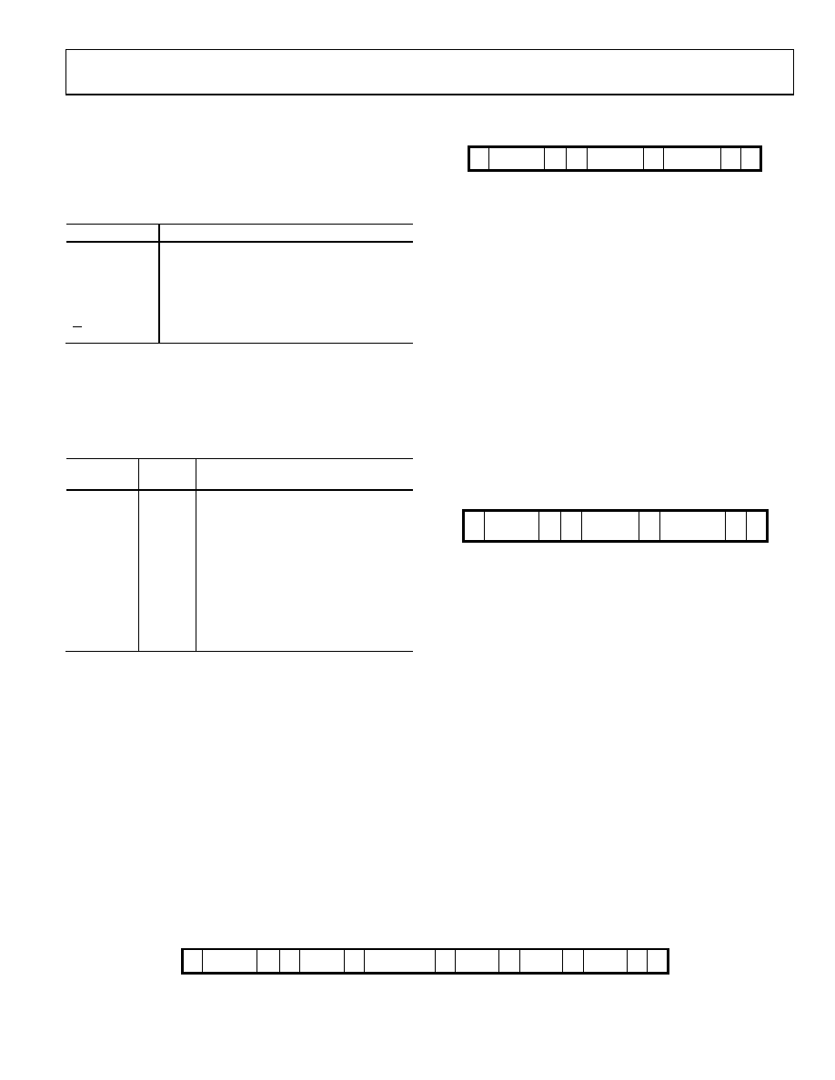
Figure 26. Writing Register Data to Register Address
In the AD5934, the write byte protocol is also used to set a
pointer to a register address (see Figure 27). This protocol is
used for a subsequent single-byte read from the same address,
block read, or block write starting at that address.
To set a register pointer, the following sequence is applied:
1. The master device asserts a start condition on SDA.
2. The master sends the 7-bit slave address followed by the
write bit (low).
3. The addressed slave device asserts an acknowledge on SDA.
4. The master sends a pointer command code (see Table 15, an
address pointer = 1011 0000).
5. The slave asserts an acknowledge on SDA.
6. The master sends a data byte (a register address to where
the pointer is to point).
7. The slave asserts an acknowledge on SDA.
8. The master asserts a stop condition on SDA to end the
transaction.
S
A
W
A
P
POINTER
COMMAND
1011 0000
SLAVE
ADDRESS
REGISTER
ADDRESS
TO POINT TO
05325-
050
Figure 27. Setting Address Pointer to Register Address
BLOCK WRITE
In this operation, the master device writes a block of data to a
slave device (see Figure 28). The start address for a block write
must previously have been set. In the case of the AD5934, this is
done by setting a pointer to set the register address.
1. The master device asserts a start condition on SDA.
2. The master sends the 7-bit slave address followed by the
write bit (low).
3. The addressed slave device asserts an acknowledge on SDA.
4. The master sends an 8-bit command code (1010 0000) that
tells the slave device to expect a block write.
5. The slave asserts an acknowledge on SDA.
6. The master sends a data byte that tells the slave device the
number of data bytes to be sent to it.
7. The slave asserts an acknowledge on SDA.
8. The master sends the data bytes.
9. The slave asserts an acknowledge on SDA after each data byte.
10. The master asserts a stop condition on SDA to end the
transaction.
A
S
W
A
P
SLAVE
ADDRESS
BLOCK
WRITE
NUMBER
BYTES WRITE
BYTE 0
BYTE 1
BYTE 2
05325-
051
Figure 28. Writing a Block Write
相关PDF资料 |
PDF描述 |
|---|---|
| BQ2057CDGK | IC LI-ION LDO CHRG MGMT 8-MSOP |
| VE-J7Y-EZ-F3 | CONVERTER MOD DC/DC 3.3V 16.5W |
| VE-J7Y-EZ-F2 | CONVERTER MOD DC/DC 3.3V 16.5W |
| MC34164P-3RPG | IC SENSOR UNDERVOLT 3V TO-226AA |
| BQ2057TSN | IC LITH-ION LDO CHRG MGMT 8-SOIC |
相关代理商/技术参数 |
参数描述 |
|---|---|
| EVAL-AD607EBZ | 功能描述:BOARD EVALUATION FOR AD607 RoHS:是 类别:RF/IF 和 RFID >> RF 评估和开发套件,板 系列:- 标准包装:1 系列:- 类型:GPS 接收器 频率:1575MHz 适用于相关产品:- 已供物品:模块 其它名称:SER3796 |
| EVAL-AD608EBZ | 功能描述:BOARD EVALUATION FOR AD608 RoHS:是 类别:RF/IF 和 RFID >> RF 评估和开发套件,板 系列:- 标准包装:1 系列:- 类型:GPS 接收器 频率:1575MHz 适用于相关产品:- 已供物品:模块 其它名称:SER3796 |
| EVAL-AD7021DBZ5 | 制造商:Analog Devices 功能描述:EVAL BOARD ((NS)) |
| EVAL-AD7091RSDZ | 功能描述:数据转换 IC 开发工具 EVALUATION BOARD RoHS:否 制造商:Texas Instruments 产品:Demonstration Kits 类型:ADC 工具用于评估:ADS130E08 接口类型:SPI 工作电源电压:- 6 V to + 6 V |
| EVAL-AD7091SDZ | 功能描述:数据转换 IC 开发工具 EVALUATION BOARD RoHS:否 制造商:Texas Instruments 产品:Demonstration Kits 类型:ADC 工具用于评估:ADS130E08 接口类型:SPI 工作电源电压:- 6 V to + 6 V |
发布紧急采购,3分钟左右您将得到回复。