- 您现在的位置:买卖IC网 > PDF目录17048 > EVAL-AD7171EBZ (Analog Devices Inc)BOARD EVAL FOR AD7171 PDF资料下载
参数资料
| 型号: | EVAL-AD7171EBZ |
| 厂商: | Analog Devices Inc |
| 文件页数: | 14/16页 |
| 文件大小: | 0K |
| 描述: | BOARD EVAL FOR AD7171 |
| 标准包装: | 1 |
| ADC 的数量: | 1 |
| 位数: | 16 |
| 采样率(每秒): | 125 |
| 数据接口: | 串行 |
| 输入范围: | ±VREF |
| 工作温度: | -40°C ~ 105°C |
| 已用 IC / 零件: | AD7171 |
| 已供物品: | 板 |
Data Sheet
AD7171
Rev. A | Page 7 of 16
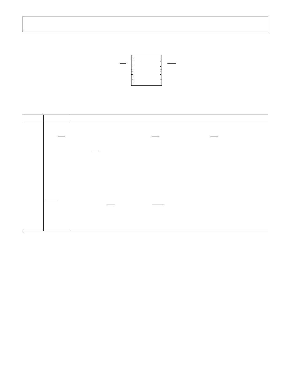
PIN CONFIGURATION AND FUNCTION DESCRIPTIONS
1
SCLK
2
DOUT/RDY
3
AIN(+)
4
AIN(–)
5
REFIN(+)
10 NC
NOTES
1. NC = NO CONNECT.
2. CONNECT EXPOSED PAD TO GROUND.
9 PDRST
8VDD
7GND
6REFIN(–)
AD7171
TOP VIEW
(Not to Scale)
08
41
7-
00
5
Figure 5. Pin Configuration
Table 5. Pin Function Descriptions
Pin No.
Mnemonic
Description
1
SCLK
Serial Clock Input. This serial clock input is for data transfers from the ADC. The SCLK has a Schmitt-triggered
input. The serial clock can be continuous with all data transmitted in a constant train of pulses. Alternatively, it
can be a noncontinuous clock with the information being transmitted from the ADC in smaller batches of data.
2
DOUT/RDY
Serial Data Output/Data Ready Output. DOUT/RDY serves a dual purpose. DOUT/RDY operates as a data ready
pin, going low to indicate the completion of a conversion. In addition, it functions as a serial data output pin to
access the data register of the ADC. Eight status bits accompany each data read. See Figure 13 for further details.
The DOUT/RDY falling edge can be used as an interrupt to a processor, indicating that new data is available. If
the data is not read after the conversion, the pin goes high before the next update occurs.
3
AIN(+)
Analog Input. AIN(+) is the positive terminal of the differential analog input pair AIN(+)/AIN().
4
AIN()
Analog Input. AIN() is the negative terminal of the dierential analog input pair AIN(+)/AIN().
5
REFIN(+)
Positive Reference Input. An external reference can be applied between REFIN(+) and REFIN(–). The nominal
reference voltage (REFIN(+) – REFIN()) is 5 V, but the part can function with a reference of 0.5 V to VDD.
6
REFIN()
Negative Reference Input.
7
GND
Ground Reference Point.
8
VDD
Supply Voltage, 2.7 V to 5.25 V.
9
PDRST
Power-Down/Reset. When this pin is low, the ADC is placed in power-down mode. All the logic on the chip is
reset and the DOUT/RDY pin is tristated. When PDRST is high, the ADC is taken out of power-down mode. The
on-chip clock powers up and settles, and the ADC continuously converts. The internal clock requires 1 ms
approximately to power up.
10
NC
This pin should be connected to GND for correct operation.
EPAD
Connect the exposed pad to ground.
相关PDF资料 |
PDF描述 |
|---|---|
| HKQ0603S3N8C-T | INDUCTOR HI FREQ 3.8NH 0201 |
| ADR441ARMZ-REEL7 | IC VREF SERIES PREC 2.5V 8-MSOP |
| ECC19DRTN-S13 | CONN EDGECARD 38POS .100 EXTEND |
| ECE-A1HKGR22 | CAP ALUM 0.22UF 50V 20% RADIAL |
| ECC31DJCN-S1136 | CONN EDGECARD 62PS .100 PRESSFIT |
相关代理商/技术参数 |
参数描述 |
|---|---|
| EVAL-AD7173-8SDZ | 制造商:Analog Devices 功能描述:EVAL BOARD MULTI CHANNEL - Boxed Product (Development Kits) |
| EVAL-AD7175-8SDZ | 功能描述:AD7175-8 - 24 Bit 250k Samples per Second Analog to Digital Converter (ADC) Evaluation Board 制造商:analog devices inc. 系列:- 零件状态:有效 A/D 转换器数:1 位数:24 采样率(每秒):250k 数据接口:并联 输入范围:±VREF 不同条件下的功率(典型值):105mW @ 250kSPS 使用的 IC/零件:AD7175-8 所含物品:板,电源 标准包装:1 |
| EVAL-AD7176-2SDZ | 功能描述:数据转换 IC 开发工具 EVAL BOARD TWO CHANNEL MUX ED ADC RoHS:否 制造商:Texas Instruments 产品:Demonstration Kits 类型:ADC 工具用于评估:ADS130E08 接口类型:SPI 工作电源电压:- 6 V to + 6 V |
| EVAL-AD7190EBZ | 功能描述:BOARD EVAL FOR AD7190 RoHS:是 类别:编程器,开发系统 >> 评估板 - 模数转换器 (ADC) 系列:- 产品培训模块:Obsolescence Mitigation Program 标准包装:1 系列:- ADC 的数量:1 位数:12 采样率(每秒):94.4k 数据接口:USB 输入范围:±VREF/2 在以下条件下的电源(标准):- 工作温度:-40°C ~ 85°C 已用 IC / 零件:MAX11645 已供物品:板,软件 |
| EVAL-AD7191EBZ | 功能描述:BOARD EVAL FOR AD7191 RoHS:是 类别:编程器,开发系统 >> 评估板 - 模数转换器 (ADC) 系列:- 产品培训模块:Obsolescence Mitigation Program 标准包装:1 系列:- ADC 的数量:1 位数:12 采样率(每秒):94.4k 数据接口:USB 输入范围:±VREF/2 在以下条件下的电源(标准):- 工作温度:-40°C ~ 85°C 已用 IC / 零件:MAX11645 已供物品:板,软件 |
发布紧急采购,3分钟左右您将得到回复。