- 您现在的位置:买卖IC网 > PDF目录17048 > EVAL-AD7171EBZ (Analog Devices Inc)BOARD EVAL FOR AD7171 PDF资料下载
参数资料
| 型号: | EVAL-AD7171EBZ |
| 厂商: | Analog Devices Inc |
| 文件页数: | 2/16页 |
| 文件大小: | 0K |
| 描述: | BOARD EVAL FOR AD7171 |
| 标准包装: | 1 |
| ADC 的数量: | 1 |
| 位数: | 16 |
| 采样率(每秒): | 125 |
| 数据接口: | 串行 |
| 输入范围: | ±VREF |
| 工作温度: | -40°C ~ 105°C |
| 已用 IC / 零件: | AD7171 |
| 已供物品: | 板 |
AD7171
Data Sheet
Rev. A | Page 10 of 16
ADC CIRCUIT INFORMATION
OVERVIEW
The AD7171 is a low power ADC that incorporates a precision
16-bit Σ-Δ modulator and an on-chip digital filter intended for
measuring wide dynamic range, low frequency signals. The
device has an internal clock and one differential input. It
operates with an output data rate of 125 Hz and has a gain of 1.
A 2-wire interface simplifies data retrieval from the AD7171.
FILTER, DATA RATE, AND SETTLING TIME
The AD7171 uses a sinc3 filter. The output data rate is set to
125 Hz; thus, valid conversions are available every 1/125 = 8 ms.
If a reset occurs, then the user must allow the complete settling
time for the first conversion after the reset. The settling time is
equal to 24 ms. Subsequent conversions are available at 125 Hz.
When a step change occurs on the analog input, the AD7171
requires several conversion cycles to generate a valid conversion.
If the step change occurs synchronous to the conversion period,
then the settling time of the AD7171 must be allowed to generate
a valid conversion. If the step change occurs asynchronous to
the end of a conversion, then an extra conversion must be allowed
to generate a valid conversion. The data register is updated with
all the conversions but, for an accurate result, the user must
allow the required time.
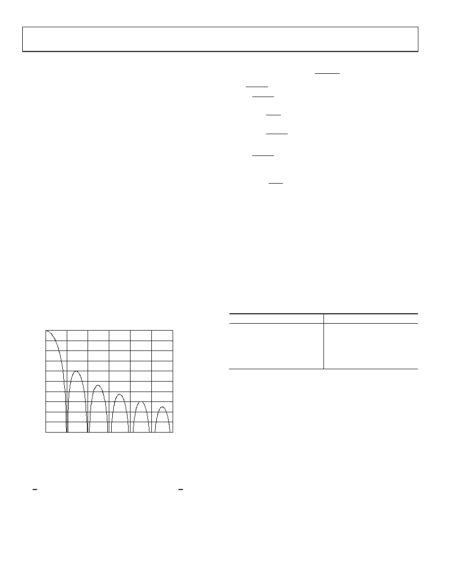
Figure 12 shows the filter response of the filter. The only external
filtering required on the analog inputs is a simple R-C filter to
provide rejection at multiples of the master clock. See Table 7
for suitable external R-C combinations.
0
–100
–90
–80
–70
–60
–50
–40
–30
–20
–10
0750
625
500
375
250
125
FI
LT
E
R
G
A
IN
(d
B
)
INPUT SIGNAL FREQUENCY (Hz)
08
417
-011
Figure 12. Filter Response
GAIN
The AD7171 has a gain of 1. The acceptable analog input range
is +VREF. Therefore, with VREF = 5 V, the input range is +5 V.
POWER-DOWN/RESET(PDRST)
The PDRST pin functions as a power-down pin and a reset pin.
When PDRST is taken low, the AD7171 is powered down. The
entire ADC is powered down (including the on-chip clock), and
the DOUT/RDY pin is tristated. The circuitry and serial interface
are also reset. This resets the logic, the digital filter, and the analog
modulator. PDRST must be held low for 100 ns minimum to
initiate the reset function (see Figure 4).
When PDRST is taken high, the AD7171 is taken out of power-
down mode. When the on-chip clock has powered up (1 ms,
typically), the modulator then begins sampling the analog input.
The DOUT/RDY pin becomes active, going high until a valid
conversion is available. A reset is automatically performed on
power-up.
ANALOG INPUT CHANNEL
The AD7171 has one differential analog input channel that is
connected to the modulator; that is, the input is unbuffered.
Note that this unbuffered input path provides a dynamic load to
the driving source. Therefore, resistor/capacitor combinations on
the input pins can cause dc gain errors, depending on the output
impedance of the source that is driving the ADC input. Table 7
shows the allowable external resistance/capacitance values such
that no gain error at the 16-bit level is introduced.
Table 7. External R-C Combination for No Gain Error
C (pF)
R (Ω)
50
9 k
100
6 k
500
1.5 k
1000
900
5000
200
The absolute input voltage range is restricted to a range between
GND 30 mV and VDD + 30 mV. Care must be taken in setting
up the common-mode voltage to avoid exceeding these limits.
Otherwise, there is degradation in linearity and noise performance.
BIPOLAR CONFIGURATION
The AD7171 accepts a bipolar input range. A bipolar input
range does not imply that the part can tolerate negative voltages
with respect to system GND. Signals on the AIN(+) input are
referenced to the voltage on the AIN() input. For example, if
AIN() is 2.5 V, the analog input range on the AIN(+) input is
0 V to 5 V when a 2.5 V reference is used.
相关PDF资料 |
PDF描述 |
|---|---|
| HKQ0603S3N8C-T | INDUCTOR HI FREQ 3.8NH 0201 |
| ADR441ARMZ-REEL7 | IC VREF SERIES PREC 2.5V 8-MSOP |
| ECC19DRTN-S13 | CONN EDGECARD 38POS .100 EXTEND |
| ECE-A1HKGR22 | CAP ALUM 0.22UF 50V 20% RADIAL |
| ECC31DJCN-S1136 | CONN EDGECARD 62PS .100 PRESSFIT |
相关代理商/技术参数 |
参数描述 |
|---|---|
| EVAL-AD7173-8SDZ | 制造商:Analog Devices 功能描述:EVAL BOARD MULTI CHANNEL - Boxed Product (Development Kits) |
| EVAL-AD7175-8SDZ | 功能描述:AD7175-8 - 24 Bit 250k Samples per Second Analog to Digital Converter (ADC) Evaluation Board 制造商:analog devices inc. 系列:- 零件状态:有效 A/D 转换器数:1 位数:24 采样率(每秒):250k 数据接口:并联 输入范围:±VREF 不同条件下的功率(典型值):105mW @ 250kSPS 使用的 IC/零件:AD7175-8 所含物品:板,电源 标准包装:1 |
| EVAL-AD7176-2SDZ | 功能描述:数据转换 IC 开发工具 EVAL BOARD TWO CHANNEL MUX ED ADC RoHS:否 制造商:Texas Instruments 产品:Demonstration Kits 类型:ADC 工具用于评估:ADS130E08 接口类型:SPI 工作电源电压:- 6 V to + 6 V |
| EVAL-AD7190EBZ | 功能描述:BOARD EVAL FOR AD7190 RoHS:是 类别:编程器,开发系统 >> 评估板 - 模数转换器 (ADC) 系列:- 产品培训模块:Obsolescence Mitigation Program 标准包装:1 系列:- ADC 的数量:1 位数:12 采样率(每秒):94.4k 数据接口:USB 输入范围:±VREF/2 在以下条件下的电源(标准):- 工作温度:-40°C ~ 85°C 已用 IC / 零件:MAX11645 已供物品:板,软件 |
| EVAL-AD7191EBZ | 功能描述:BOARD EVAL FOR AD7191 RoHS:是 类别:编程器,开发系统 >> 评估板 - 模数转换器 (ADC) 系列:- 产品培训模块:Obsolescence Mitigation Program 标准包装:1 系列:- ADC 的数量:1 位数:12 采样率(每秒):94.4k 数据接口:USB 输入范围:±VREF/2 在以下条件下的电源(标准):- 工作温度:-40°C ~ 85°C 已用 IC / 零件:MAX11645 已供物品:板,软件 |
发布紧急采购,3分钟左右您将得到回复。