- 您现在的位置:买卖IC网 > PDF目录17048 > EVAL-AD7276SDZ (Analog Devices Inc)BOARD EVAL FOR AD7276 PDF资料下载
参数资料
| 型号: | EVAL-AD7276SDZ |
| 厂商: | Analog Devices Inc |
| 文件页数: | 9/29页 |
| 文件大小: | 0K |
| 描述: | BOARD EVAL FOR AD7276 |
| 标准包装: | 1 |
| ADC 的数量: | 1 |
| 位数: | 12 |
| 采样率(每秒): | 3M |
| 数据接口: | 串行 |
| 输入范围: | 0 ~ 3.6 V |
| 在以下条件下的电源(标准): | 19.8mW @ 3MSPS,3.6 V |
| 工作温度: | -40°C ~ 125°C |
| 已用 IC / 零件: | AD7276 |
| 已供物品: | 板 |
第1页第2页第3页第4页第5页第6页第7页第8页当前第9页第10页第11页第12页第13页第14页第15页第16页第17页第18页第19页第20页第21页第22页第23页第24页第25页第26页第27页第28页第29页
AD7276/AD7277/AD7278
Rev. C | Page 16 of 28
THEORY OF OPERATION
CIRCUIT INFORMATION
The AD7276/AD7277/AD7278 are fast, micropower, 12-/10-/
8-bit, single-supply ADCs, respectively. The parts can be operated
from a 2.35 V to 3.6 V supply. When operated from a supply
voltage within this range, the AD7276/AD7277/AD7278 are
capable of throughput rates of 3 MSPS when provided with a
48 MHz clock.
The AD7276/AD7277/AD7278 provide the user with an on-
chip track-and-hold ADC and a serial interface housed in a tiny
6-lead TSOT or an 8-lead MSOP package, which offers the user
considerable space-saving advantages over alternative solutions.
The serial clock input accesses data from the part and provides
the clock source for the successive approximation ADC. The
analog input range is 0 V to VDD. An external reference is not
required for the ADC, and there is no reference on-chip. The
reference for the AD7276/AD7277/AD7278 is derived from the
power supply, resulting in the widest dynamic input range.
The AD7276/AD7277/AD7278 also feature a power-down
option to save power between conversions. The power-down
feature is implemented across the standard serial interface as
described in the Modes of Operation section.
CONVERTER OPERATION
The AD7276/AD7277/AD7278 are successive approximation
ADCs that are based on a charge redistribution DAC. Figure 19
shows the ADC during its acquisition phase, where SW2 is closed,
SW1 is in Position A, the comparator is held in a balanced con-
dition, and the sampling capacitor acquires the signal on VIN.
04
90
3-
0
19
COMPARATOR
ACQUISITION
PHASE
VDD/2
SW2
VIN
SAMPLING
CAPACITOR
AGND
A
SW1
B
CHARGE
REDISTRIBUTION
DAC
CONTROL
LOGIC
Figure 19. ADC Acquisition Phase
When the ADC starts a conversion, SW2 opens and SW1 moves
to Position B, causing the comparator to become unbalanced
(see Figure 20). The control logic and the charge redistribution
DACs are used to add and subtract fixed amounts of charge
from the sampling capacitor to bring the comparator back into
a balanced condition. When the comparator is rebalanced, the
conversion is complete. The control logic generates the ADC
output code.
04
90
3-
0
20
COMPARATOR
ACQUISITION
PHASE
VDD/2
SW2
VIN
SAMPLING
CAPACITOR
AGND
A
SW1
B
CHARGE
REDISTRIBUTION
DAC
CONTROL
LOGIC
Figure 20. ADC Conversion Phase
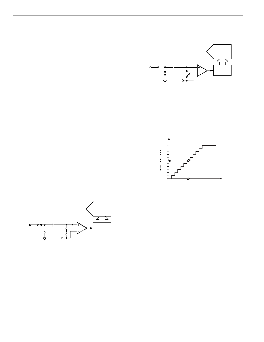
ADC TRANSFER FUNCTION
The output coding of the AD7276/AD7277/AD7278 is straight
binary. The designed code transitions occur midway between
successive integer LSB values, such as 0.5 LSB and 1.5 LSB. The
LSB size is VDD/4,096 for the AD7276, VDD/1,024 for the AD7277,
and VDD/256 for the AD7278. The ideal transfer characteristic
for the AD7276/AD7277/AD7278 is shown in Figure 21.
04
90
3-
0
21
000...000
0V
ADC
CO
DE
ANALOG INPUT
111...111
000...001
111...000
011...111
111...110
000...010
1LSB = VREF/4096 (AD7276)
1LSB = VREF/1024 (AD7277)
1LSB = VREF/256 (AD7278)
+VDD – 1.5LSB
0.5LSB
Figure 21. AD7276/AD7277/AD7278 Transfer Characteristics
TYPICAL CONNECTION DIAGRAM
Figure 22 shows a typical connection diagram for the AD7276/
AD7277/AD7278. VREF is taken internally from VDD; therefore,
VDD should be decoupled. This provides an analog input range
of 0 V to VDD. The conversion result is output in a 16-bit word
with two leading zeros followed by the 12-bit, 10-bit, or 8-bit
result. The 12-bit result from the AD7276 is followed by two
trailing zeros; the 10-bit and 8-bit results from the AD7277 and
AD7278 are followed by four and six trailing zeros, respectively.
Alternatively, because the supply current required by the AD7276/
AD7277/AD7278 is so low, a precision reference can be used as the
supply source for the AD7276/AD7277/AD7278. A REF19x voltage
reference (REF193 for 3 V) can be used to supply the required
voltage to the ADC (see Figure 22). This configuration is especially
useful if the power supply is noisy or the system’s supply voltage is a
value other than 3 V (for example, 5 V or 15 V). The REF19x
outputs a steady voltage to the AD7276/AD7277/AD7278. If the
low dropout REF193 is used, it must supply a current of typically
1 mA to the AD7276/AD7277/AD7278. When the ADC is
converting at a rate of 3 MSPS, the REF193 must supply a maxi-
mum of 5 mA to the AD7276/AD7277/AD7278.
相关PDF资料 |
PDF描述 |
|---|---|
| ABC05DRYS | CONN EDGECARD 10POS .100 DIP SLD |
| ESC06DREI-S734 | CONN EDGECARD 12POS .100 EYELET |
| EBC12DREI-S734 | CONN EDGECARD 24POS .100 EYELET |
| ABC07DRXN | CONN EDGECARD 14POS .100 DIP SLD |
| 0210490903 | CABLE JUMPER 1.25MM .076M 21POS |
相关代理商/技术参数 |
参数描述 |
|---|---|
| EVAL-AD7277CB | 制造商:Analog Devices 功能描述:EVAL BD 3 MSPS, 12-/10-/8BIT ADCS IN 6-LEAD TSOT - Bulk |
| EVAL-AD7280AEDZ | 功能描述:BOARD EVAL FOR AD7280 RoHS:是 类别:编程器,开发系统 >> 评估演示板和套件 系列:- 标准包装:1 系列:PSoC® 主要目的:电源管理,热管理 嵌入式:- 已用 IC / 零件:- 主要属性:- 次要属性:- 已供物品:板,CD,电源 |
| EVAL-AD7291SDZ | 功能描述:BOARD EVAL FOR AD7291 RoHS:是 类别:编程器,开发系统 >> 评估板 - 模数转换器 (ADC) 系列:- 产品培训模块:Obsolescence Mitigation Program 标准包装:1 系列:- ADC 的数量:1 位数:12 采样率(每秒):94.4k 数据接口:USB 输入范围:±VREF/2 在以下条件下的电源(标准):- 工作温度:-40°C ~ 85°C 已用 IC / 零件:MAX11645 已供物品:板,软件 |
| EVAL-AD7292SDZ | 功能描述:数据转换 IC 开发工具 EVALUATION BOARD RoHS:否 制造商:Texas Instruments 产品:Demonstration Kits 类型:ADC 工具用于评估:ADS130E08 接口类型:SPI 工作电源电压:- 6 V to + 6 V |
| EVAL-AD7294EBZ | 功能描述:BOARD EVALUATION FOR AD7294 RoHS:是 类别:编程器,开发系统 >> 评估板 - 模数转换器 (ADC) 系列:- 产品培训模块:Obsolescence Mitigation Program 标准包装:1 系列:- ADC 的数量:1 位数:12 采样率(每秒):94.4k 数据接口:USB 输入范围:±VREF/2 在以下条件下的电源(标准):- 工作温度:-40°C ~ 85°C 已用 IC / 零件:MAX11645 已供物品:板,软件 |
发布紧急采购,3分钟左右您将得到回复。