- 您现在的位置:买卖IC网 > PDF目录17056 > EVAL-AD7321CBZ (Analog Devices Inc)BOARD EVALUATION FOR AD7321 PDF资料下载
参数资料
| 型号: | EVAL-AD7321CBZ |
| 厂商: | Analog Devices Inc |
| 文件页数: | 1/37页 |
| 文件大小: | 0K |
| 描述: | BOARD EVALUATION FOR AD7321 |
| 标准包装: | 1 |
| 系列: | iCMOS® |
| ADC 的数量: | 1 |
| 位数: | 12 |
| 采样率(每秒): | 500k |
| 数据接口: | 串行 |
| 输入范围: | ±10 V |
| 在以下条件下的电源(标准): | 17mW @ 500kSPS |
| 工作温度: | -40°C ~ 85°C |
| 已用 IC / 零件: | AD7321 |
| 已供物品: | 板,CD |
| 相关产品: | AD7321BRUZ-REEL-ND - IC ADC 12BIT+SAR 2CHAN 14-TSSOP AD7321BRUZ-REEL7-ND - IC ADC 12BIT+ SAR 2CHAN 14TSSOP AD7321BRUZ-ND - IC ADC 12BIT+ SAR 2CHAN 14TSSOP |
当前第1页第2页第3页第4页第5页第6页第7页第8页第9页第10页第11页第12页第13页第14页第15页第16页第17页第18页第19页第20页第21页第22页第23页第24页第25页第26页第27页第28页第29页第30页第31页第32页第33页第34页第35页第36页第37页
500 kSPS, 2-Channel, Software-Selectable,
True Bipolar Input, 12-Bit Plus Sign ADC
Data Sheet
Rev. B
Information furnished by Analog Devices is believed to be accurate and reliable. However, no
responsibilityisassumedbyAnalogDevicesforitsuse,norforanyinfringementsofpatentsorother
rightsofthirdpartiesthatmayresultfromitsuse.Specificationssubjecttochangewithoutnotice.No
license is granted by implication or otherwise under any patent or patent rights of Analog Devices.
Trademarksandregisteredtrademarksarethepropertyoftheirrespectiveowners.
One Technology Way, P.O. Box 9106, Norwood, MA 02062-9106, U.S.A.
Tel: 781.329.4700
2006–2013 Analog Devices, Inc. All rights reserved.
FEATURES
12-bit plus sign SAR ADC
True bipolar input ranges
Software-selectable input ranges
±10 V, ±5 V, ±2.5 V, 0 V to +10 V
500 kSPS throughput rate
2 analog input channels with channel sequencer
Single-ended, true differential, and pseudo differential
analog input capability
High analog input impedance
Low power: 18 mW
Full power signal bandwidth: 22 MHz
Internal 2.5 V reference
High speed serial interface
Power-down modes
14-lead TSSOP package
i
CMOS process technology
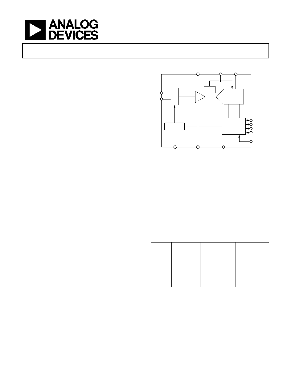
FUNCTIONAL BLOCK DIAGRAM
VIN0
DOUT
SCLK
CS
DIN
VDRIVE
VIN1
VDD
REFIN/OUT
VCC
AGND
VSS
DGND
CONTROL LOGIC
AND REGISTERS
13-BIT
SUCCESSIVE
APPROXIMATION
ADC
T/H
2.5V
VREF
I/P
MUX
CHANNEL
SEQUENCER
AD7321
05399-
001
Figure 1.
GENERAL DESCRIPTION
approximation ADC designed on the iCMOS (industrial
CMOS) process. iCMOS is a process combining high voltage
silicon with submicron CMOS and complementary bipolar
technologies. It enables the development of a wide range of high
performance analog ICs capable of 33 V operation in a footprint
that no previous generation of high voltage parts could achieve.
Unlike analog ICs using conventional CMOS processes, iCMOS
components can accept bipolar input signals while providing
increased performance, dramatically reduced power consumption,
and reduced package size.
The AD7321 can accept true bipolar analog input signals. The
AD7321 has four software-selectable input ranges, ±10 V, ±5 V,
±2.5 V, and 0 V to +10 V. Each analog input channel is indepen-
dently programmed to one of the four input ranges. The analog
input channels on the AD7321 are programmed to be single-ended,
true differential, or pseudo differential.
The ADC contains a 2.5 V internal reference. The AD7321 also
allows for external reference operation. If a 3 V reference is applied
to the REFIN/OUT pin, the AD7321 can accept a true bipolar
±12 V analog input. A minimum of ±12 V VDD and VSS supplies
are required for the ±12 V input range. The ADC has a high speed
serial interface that can operate at throughput rates up to 500 kSPS.
PRODUCT HIGHLIGHTS
1. The AD7321 can accept true bipolar analog input signals,
±10 V, ±5 V, ±2.5 V, and 0 V to +10 V unipolar signals.
2. The two analog inputs are configured as two single-ended
inputs, one true differential input pair, or one pseudo
differential input.
3. A 500 kSPS serial interface. SPI-/QSPI-/DSP-/
MICROWIRE-compatible interface.
4. Low power, 18 mW, at a maximum throughput rate of
500 kSPS.
5. Channel sequencer.
Table 1. Similar Devices
Device
Number
Throughput
Rate
Number of bits
Number of
Channels
1000 kSPS
12-bit plus sign
8
1000 kSPS
12-bit plus sign
8
500 kSPS
12-bit plus sign
8
1000 kSPS
12-bit plus sign
4
500 kSPS
12-bit plus sign
4
1000 kSPS
12-bit plus sign
2
1
Protected by U.S. Patent No. 6,731,232.
相关PDF资料 |
PDF描述 |
|---|---|
| AD9714-DPG2-EBZ | ADC 8BIT DUAL 40LFCSP |
| EBA15DCBT | CONN EDGECARD 30POS R/A .125 SLD |
| EEM28DTKD | CONN EDGECARD 56POS DIP .156 SLD |
| EBA24DCBN | CONN EDGECARD 48POS R/A .125 SLD |
| EBM11DSEF | CONN EDGECARD 22POS .156 EYELET |
相关代理商/技术参数 |
参数描述 |
|---|---|
| EVAL-AD7322CB1 | 制造商:ATMEL 制造商全称:ATMEL Corporation 功能描述:Software Selectable True Bipolar Input, 2-Channel, 12-Bit Plus Sign ADC |
| EVAL-AD7322CBZ | 功能描述:BOARD EVALUATION FOR AD7322 RoHS:是 类别:编程器,开发系统 >> 评估板 - 模数转换器 (ADC) 系列:iCMOS® 产品培训模块:Obsolescence Mitigation Program 标准包装:1 系列:- ADC 的数量:1 位数:12 采样率(每秒):94.4k 数据接口:USB 输入范围:±VREF/2 在以下条件下的电源(标准):- 工作温度:-40°C ~ 85°C 已用 IC / 零件:MAX11645 已供物品:板,软件 |
| EVAL-AD7323CB | 制造商:AD 制造商全称:Analog Devices 功能描述:500 kSPS, 4-Channel, Software-Selectable, True Bipolar Input, 12-Bit Plus Sign ADC |
| EVAL-AD7323CBZ | 功能描述:BOARD EVALUATION FOR AD7323CBZ RoHS:是 类别:编程器,开发系统 >> 评估板 - 模数转换器 (ADC) 系列:iCMOS® 产品培训模块:Obsolescence Mitigation Program 标准包装:1 系列:- ADC 的数量:1 位数:12 采样率(每秒):94.4k 数据接口:USB 输入范围:±VREF/2 在以下条件下的电源(标准):- 工作温度:-40°C ~ 85°C 已用 IC / 零件:MAX11645 已供物品:板,软件 |
| EVAL-AD7324CB | 制造商:AD 制造商全称:Analog Devices 功能描述:4-Channel, Software-Selectable, True Bipolar Input, 12-Bit Plus Sign ADC |
发布紧急采购,3分钟左右您将得到回复。