- 您现在的位置:买卖IC网 > PDF目录17056 > EVAL-AD7321CBZ (Analog Devices Inc)BOARD EVALUATION FOR AD7321 PDF资料下载
参数资料
| 型号: | EVAL-AD7321CBZ |
| 厂商: | Analog Devices Inc |
| 文件页数: | 28/37页 |
| 文件大小: | 0K |
| 描述: | BOARD EVALUATION FOR AD7321 |
| 标准包装: | 1 |
| 系列: | iCMOS® |
| ADC 的数量: | 1 |
| 位数: | 12 |
| 采样率(每秒): | 500k |
| 数据接口: | 串行 |
| 输入范围: | ±10 V |
| 在以下条件下的电源(标准): | 17mW @ 500kSPS |
| 工作温度: | -40°C ~ 85°C |
| 已用 IC / 零件: | AD7321 |
| 已供物品: | 板,CD |
| 相关产品: | AD7321BRUZ-REEL-ND - IC ADC 12BIT+SAR 2CHAN 14-TSSOP AD7321BRUZ-REEL7-ND - IC ADC 12BIT+ SAR 2CHAN 14TSSOP AD7321BRUZ-ND - IC ADC 12BIT+ SAR 2CHAN 14TSSOP |
第1页第2页第3页第4页第5页第6页第7页第8页第9页第10页第11页第12页第13页第14页第15页第16页第17页第18页第19页第20页第21页第22页第23页第24页第25页第26页第27页当前第28页第29页第30页第31页第32页第33页第34页第35页第36页第37页
Data Sheet
AD7321
Rev. B | Page 33 of 36
APPLICATION HINTS
LAYOUT AND GROUNDING
The printed circuit board that houses the AD7321 should be
designed so that the analog and digital sections are confined to
certain areas of the board. This design facilitates the use of
ground planes that can easily be separated.
To provide optimum shielding for ground planes, a minimum
etch technique is generally best. All AGND pins on the AD7321
should be connected to the AGND plane. Digital and analog
ground pins should be joined in only one place. If the AD7321
is in a system where multiple devices require an AGND and
DGND connection, the connection should still be made at only
one point. A star point should be established as close as possible
to the ground pins on the AD7321.
Good connections should be made to the power and ground
planes. This is done with a single via or multiple vias for each
supply and ground pin.
Avoid running digital lines under the AD7321 device because
this couples noise onto the die. However, the analog ground
plane should be allowed to run under the AD7321 to avoid
noise coupling. The power supply lines to the AD7321 device
should use as large a trace as possible to provide low impedance
paths and reduce the effects of glitches on the power supply line.
To avoid radiating noise to other sections of the board, com-
ponents, such as clocks, with fast switching signals should be
shielded with digital ground and never run near the analog inputs.
Avoid crossover of digital and analog signals. To reduce the effects
of feedthrough within the board, traces should be run at right
angles to each other. A microstrip technique is the best method,
but its use may not be possible with a double-sided board. In
this technique, the component side of the board is dedicated
to ground planes, and signals are placed on the other side.
Good decoupling is also important. All analog supplies should
be decoupled with 10 F tantalum capacitors in parallel with
0.1 F capacitors to AGND. To achieve the best results from
these decoupling components, they must be placed as close as
possible to the device, ideally right up against the device. The
0.1 F capacitors should have a low effective series resistance
(ESR) and low effective series inductance (ESI), such as is
typical of common ceramic and surface mount types of
capacitors. These low ESR, low ESI capacitors provide a low
impedance path to ground at high frequencies to handle
transient currents due to internal logic switching.
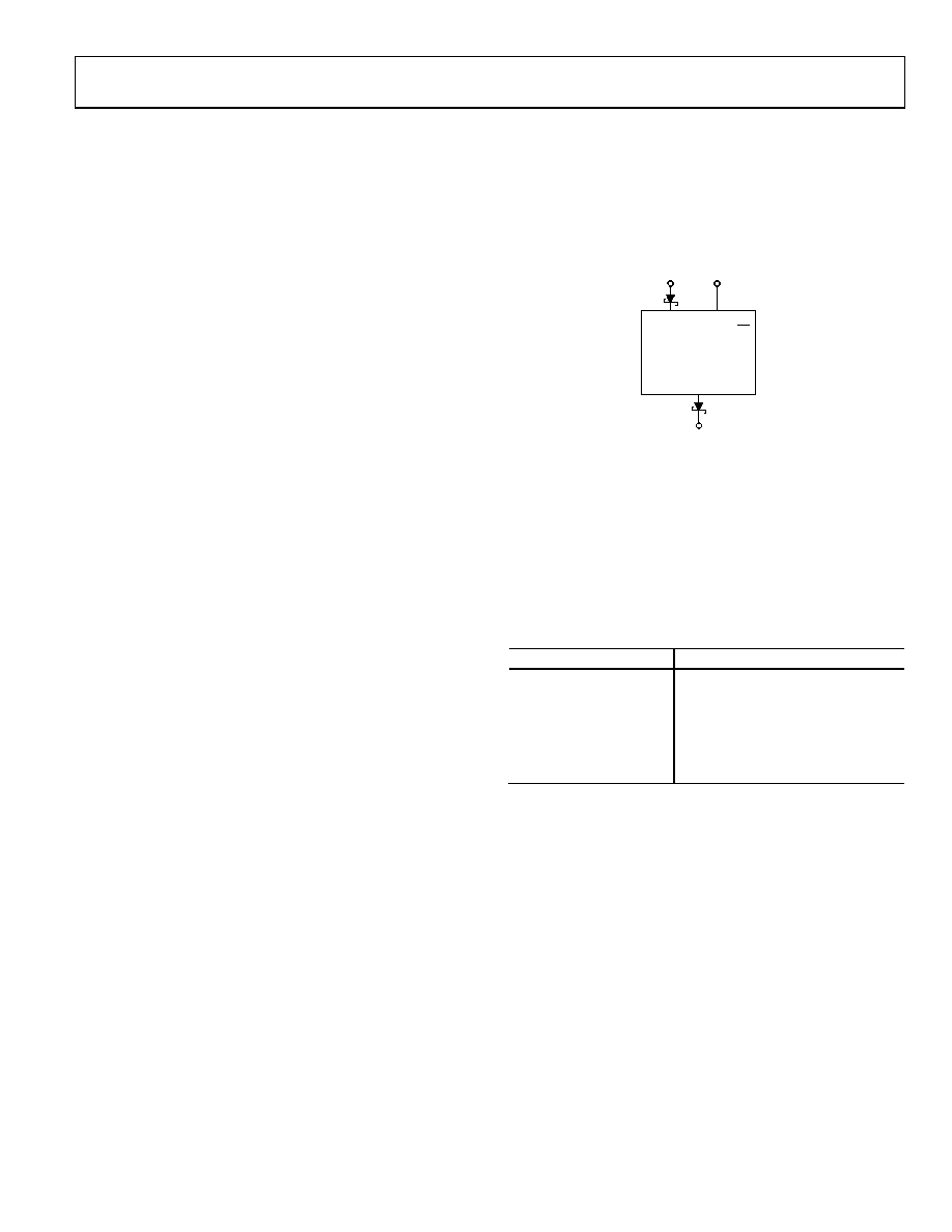
POWER SUPPLY CONFIGURATION
It is recommended that Schottky diodes be placed in series with
Schottky diode configuration. BAT43 Schottky diodes are used.
VIN0
VIN1
VDD
VSS
V+
V–
CS
SCLK
DOUT
DIN
VCC
3V/5V
NOTES
1. ADDITIONAL PINS
OMITTED FOR CLARITY.
AD7321
05399-
066
Figure 53. Schottky Diode Connection
In an application where non-symmetrical VDD and VSS supplies
are being used, adhere to the following guidelines. Table 16
outlines the VSS supply range that can be used for particular VDD
voltages when non-symmetrical supplies are required. When
recommended that these supplies be symmetrical.
Table 16. Non-Symmetrical VDD and VSS Requirements
VDD
Typical VSS Range
5 V
5 V to 5.5 V
6 V
5 V to 8.5 V
7 V
5 V to 11.5 V
8 V
5 V to 15 V
9 V
5 V to 16.5 V
10 V to 16.5 V
5 V to 16.5 V
For the 0 to 4 × VREF range, VSS can be tied to AGND as per
minimum supply recommendations outlined in Table 6.
相关PDF资料 |
PDF描述 |
|---|---|
| AD9714-DPG2-EBZ | ADC 8BIT DUAL 40LFCSP |
| EBA15DCBT | CONN EDGECARD 30POS R/A .125 SLD |
| EEM28DTKD | CONN EDGECARD 56POS DIP .156 SLD |
| EBA24DCBN | CONN EDGECARD 48POS R/A .125 SLD |
| EBM11DSEF | CONN EDGECARD 22POS .156 EYELET |
相关代理商/技术参数 |
参数描述 |
|---|---|
| EVAL-AD7322CB1 | 制造商:ATMEL 制造商全称:ATMEL Corporation 功能描述:Software Selectable True Bipolar Input, 2-Channel, 12-Bit Plus Sign ADC |
| EVAL-AD7322CBZ | 功能描述:BOARD EVALUATION FOR AD7322 RoHS:是 类别:编程器,开发系统 >> 评估板 - 模数转换器 (ADC) 系列:iCMOS® 产品培训模块:Obsolescence Mitigation Program 标准包装:1 系列:- ADC 的数量:1 位数:12 采样率(每秒):94.4k 数据接口:USB 输入范围:±VREF/2 在以下条件下的电源(标准):- 工作温度:-40°C ~ 85°C 已用 IC / 零件:MAX11645 已供物品:板,软件 |
| EVAL-AD7323CB | 制造商:AD 制造商全称:Analog Devices 功能描述:500 kSPS, 4-Channel, Software-Selectable, True Bipolar Input, 12-Bit Plus Sign ADC |
| EVAL-AD7323CBZ | 功能描述:BOARD EVALUATION FOR AD7323CBZ RoHS:是 类别:编程器,开发系统 >> 评估板 - 模数转换器 (ADC) 系列:iCMOS® 产品培训模块:Obsolescence Mitigation Program 标准包装:1 系列:- ADC 的数量:1 位数:12 采样率(每秒):94.4k 数据接口:USB 输入范围:±VREF/2 在以下条件下的电源(标准):- 工作温度:-40°C ~ 85°C 已用 IC / 零件:MAX11645 已供物品:板,软件 |
| EVAL-AD7324CB | 制造商:AD 制造商全称:Analog Devices 功能描述:4-Channel, Software-Selectable, True Bipolar Input, 12-Bit Plus Sign ADC |
发布紧急采购,3分钟左右您将得到回复。