- 您现在的位置:买卖IC网 > PDF目录17060 > EVAL-AD7356EDZ (Analog Devices Inc)BOARD EVAL AD7356 PDF资料下载
参数资料
| 型号: | EVAL-AD7356EDZ |
| 厂商: | Analog Devices Inc |
| 文件页数: | 9/21页 |
| 文件大小: | 0K |
| 描述: | BOARD EVAL AD7356 |
| 标准包装: | 1 |
| ADC 的数量: | 2 |
| 位数: | 12 |
| 采样率(每秒): | 5M |
| 数据接口: | 串行 |
| 输入范围: | ±VREF/2 |
| 在以下条件下的电源(标准): | 36mW @ 5MSPS |
| 工作温度: | -40°C ~ 85°C |
| 已用 IC / 零件: | AD7356 |
| 已供物品: | 板,CD |
AD7356
Rev. A | Page 16 of 20
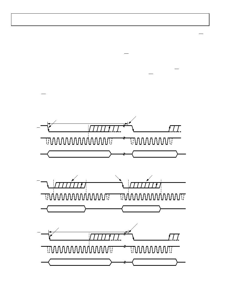
FULL POWER-DOWN MODE
Full power-down mode is intended for use in applications
where throughput rates slower than those in partial power-
down mode are required because power-up from a full power-
down takes substantially longer than that from a partial power-
down. This mode is more suited to applications in which a
series of conversions performed at a relatively high throughput
rate are followed by a long period of inactivity and, thus, power-
down. When the AD7356 is in full power-down mode, all
analog circuitry is powered down including the on-chip
reference and reference buffers. Full power-down mode is
entered in a similar way as partial power-down mode, except
that the timing sequence shown in Figure 25 must be executed
twice. The conversion process must be interrupted in a similar
fashion by bringing CS high anywhere after the second falling
edge of SCLK and before the 10th falling edge of SCLK. The
device enters partial power-down mode at this point.
To reach full power-down, the next conversion cycle must be
interrupted in the same way, as shown in Figure 27. When CS is
brought high in this window of SCLKs, the part fully powers
down.
Note that it is not necessary to complete the 14 or 16 SCLKs
once CS has been brought high to enter a power-down mode.
To exit full power-down mode and power-up the AD7356,
perform a dummy conversion, similar to powering up from
partial power-down. On the falling edge of CS, the device begins
to power up as long as CS is held low until after the falling edge
of the 10th SCLK. The required power-up time must elapse
before a conversion can be initiated, as shown in
.
SCLK
CS
SDATAA
SDATAB
INVALID DATA
VALID DATA
110
14
1
THE PART BEGINS
TO POWER UP.
tPOWER-UP1
0
650
5-
02
0
THE PART IS FULLY POWERED UP;
SEE THE POWER-UP TIMES SECTION.
Figure 26. Exiting Partial Power-Down Mode
THREE-STATE
110
14
2
SCLK
CS
SDATAA
SDATAB
THREE-STATE
110
2
INVALID DATA
THE PART BEGINS
TO POWER UP.
THE PART ENTERS
PARTIAL POWER-DOWN MODE.
THE PART ENTERS
FULL POWER-DOWN MODE.
14
06
50
5-
02
1
Figure 27. Entering Full Power-Down Mode
SCLK
SDATAA
SDATAB
INVALID DATA
VALID DATA
1
10
14
1
THE PART BEGINS
TO POWER UP.
THE PART IS FULLY POWERED UP;
SEE THE POWER-UP TIMES SECTION.
tPOWER-UP2
CS
06
50
5-
0
22
Figure 28. Exiting Full Power-Down Mode
相关PDF资料 |
PDF描述 |
|---|---|
| MIC2009YM6 TR | IC DISTRIBUTION SW ADJ SOT23-6 |
| 0210391030 | CABLE JUMPER 1MM .030M 33POS |
| EVAL-AD7352EDZ | BOARD EVAL AD7352 |
| 0210390949 | CABLE JUMPER 1MM .102M 25POS |
| 0210390948 | CABLE JUMPER 1MM .102M 25POS |
相关代理商/技术参数 |
参数描述 |
|---|---|
| EVAL-AD7357EDZ | 功能描述:BOARD EVAL FOR AD7357 RoHS:是 类别:编程器,开发系统 >> 评估板 - 模数转换器 (ADC) 系列:- 产品培训模块:Obsolescence Mitigation Program 标准包装:1 系列:- ADC 的数量:1 位数:12 采样率(每秒):94.4k 数据接口:USB 输入范围:±VREF/2 在以下条件下的电源(标准):- 工作温度:-40°C ~ 85°C 已用 IC / 零件:MAX11645 已供物品:板,软件 |
| EVAL-AD7366CBZ | 功能描述:BOARD EVALUATION FOR AD7366 RoHS:是 类别:编程器,开发系统 >> 评估板 - 模数转换器 (ADC) 系列:iCMOS® 产品培训模块:Obsolescence Mitigation Program 标准包装:1 系列:- ADC 的数量:1 位数:12 采样率(每秒):94.4k 数据接口:USB 输入范围:±VREF/2 在以下条件下的电源(标准):- 工作温度:-40°C ~ 85°C 已用 IC / 零件:MAX11645 已供物品:板,软件 |
| EVAL-AD7366SDZ | 功能描述:BOARD EVAL FOR AD7366 RoHS:是 类别:编程器,开发系统 >> 评估板 - 模数转换器 (ADC) 系列:iCMOS® 产品培训模块:Obsolescence Mitigation Program 标准包装:1 系列:- ADC 的数量:1 位数:12 采样率(每秒):94.4k 数据接口:USB 输入范围:±VREF/2 在以下条件下的电源(标准):- 工作温度:-40°C ~ 85°C 已用 IC / 零件:MAX11645 已供物品:板,软件 |
| EVAL-AD7367CBZ | 制造商:AD 制造商全称:Analog Devices 功能描述:True Bipolar Input, Dual 1 レs, 12-/14-Bit, 2-Channel SAR ADCs |
| EVAL-AD7367SDZ | 功能描述:数据转换 IC 开发工具 EVALUATION CONTROL BOARD I.C. RoHS:否 制造商:Texas Instruments 产品:Demonstration Kits 类型:ADC 工具用于评估:ADS130E08 接口类型:SPI 工作电源电压:- 6 V to + 6 V |
发布紧急采购,3分钟左右您将得到回复。