- 您现在的位置:买卖IC网 > PDF目录17056 > EVAL-AD7366CBZ (Analog Devices Inc)BOARD EVALUATION FOR AD7366 PDF资料下载
参数资料
| 型号: | EVAL-AD7366CBZ |
| 厂商: | Analog Devices Inc |
| 文件页数: | 2/29页 |
| 文件大小: | 0K |
| 描述: | BOARD EVALUATION FOR AD7366 |
| 标准包装: | 1 |
| 系列: | iCMOS® |
| ADC 的数量: | 2 |
| 位数: | 12 |
| 采样率(每秒): | 1M |
| 数据接口: | 串行 |
| 输入范围: | ±10 V |
| 在以下条件下的电源(标准): | 70mW @ 1MSPS |
| 工作温度: | -40°C ~ 85°C |
| 已用 IC / 零件: | AD7366 |
| 已供物品: | 板 |
| 相关产品: | AD7366BRUZ-5-ND - IC ADC 12BIT DUAL 500KSPS 24-TSS AD7366BRUZ-5500RL7-ND - IC ADC 12BIT DUAL BIPO 24-TSSOP AD7366BRUZ-5-RL7-ND - IC ADC 12BIT DUAL BIPO 24-TSSOP AD7366BRUZ-ND - IC ADC 12BIT SAR 1MSPS 24TSSOP AD7366BRUZ-RL7-ND - IC ADC 12BIT SAR 1MSPS 24TSSOP AD7366BRUZ-500RL7-ND - IC ADC 12BIT SAR 1MSPS 24TSSOP |
第1页当前第2页第3页第4页第5页第6页第7页第8页第9页第10页第11页第12页第13页第14页第15页第16页第17页第18页第19页第20页第21页第22页第23页第24页第25页第26页第27页第28页第29页
AD7366/AD7367
Rev. D | Page 9 of 28
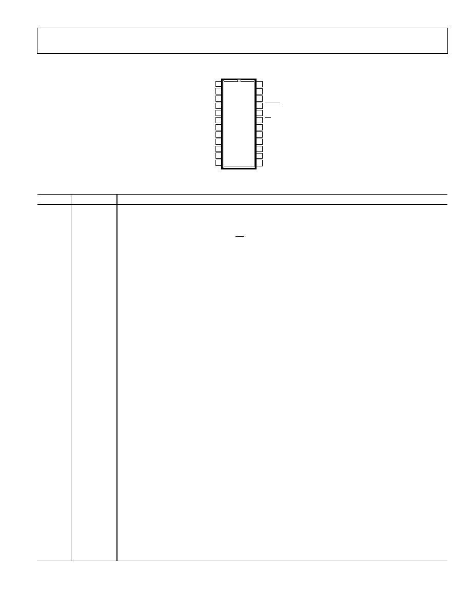
PIN CONFIGURATION AND FUNCTION DESCRIPTIONS
DOUTA 1
2
3
ADDR
4
DGND
24
23
BUSY
22
CNVST
21
RANGE0
5
RANGE1
6
AGND
7
SCLK
20
CS
19
REFSEL
18
8
AGND
17
9
16
10
15
11
14
12
13
AD7366/
AD7367
TOP VIEW
(Not to Scale)
DOUTB
DCAPA
DCAPB
DVCC
AVCC
VSS
VA1
VA2
VB1
VB2
VDD
VDRIVE
06703-
002
Figure 2. Pin Configuration
Table 6. Pin Function Descriptions
Pin No.
Mnemonic
Description
1, 23
D
OUTA, DOUTB
Serial Data Outputs. The data output is supplied to each pin as a serial data stream. The bits are clocked out on
the falling edge of the SCLK input; 12 SCLK cycles are required to access a result from the AD7366, and 14 SCLK
cycles are required for the AD7367. The data simultaneously appears on both pins from the simultaneous con-
versions of both ADCs. The data stream consists of the 12 bits of conversion data for the AD7366 and 14 bits for
the AD7367 and is provided MSB first. If CS is held low for a further 14 SCLK cycles, on either DOUTA or DOUTB, the
data from the other ADC follows on that D
OUT pin. Note, the second serial result from the AD7366 is preceeded
by two zeros. Therfore data from a simultaneous conversion on both ADCs can be gathered in serial format on
either D
2
V
DRIVE
Logic Power Supply Input. The voltage supplied at this pin determines at what voltage the interface operates.
This pin should be decoupled to DGND. The voltage range on this pin is 2.7 V to 5.25 V and may be different
from the voltage at AV
CC and DVCC, but should never exceed either by more than 0.3 V. To achieve a throughput
rate of 1.12 MSPS for the AD7366 or 1 MSPS for the AD7367, V
DRIVE must be ≥ 4.75 V.
3
DV
CC
Digital Supply Voltage, 4.75 V to 5.25 V. The DV
CC and AVCC voltages should ideally be at the same potential.
For best performance, it is recommended that the DV
CC and AVCC pins be shorted together, to ensure that the
voltage difference between them never exceeds 0.3 V even on a transient basis. This supply should be decoupled
to DGND. Place 10 F and 100 nF decoupling capacitors on the DV
CC pin.
4, 5
RANGE1,
RANGE0
Analog Input Range Selection, Logic Inputs. The polarity on these pins determines the input range of the analog
input channels. See the Analog Inputs section and Table 8 for details.
6
ADDR
Multiplexer Select, Logic Input. This input is used to select the pair of channels to be simultaneously converted,
either Channel 1 of both ADC A and ADC B, or Channel 2 of both ADC A and ADC B. The logic state on this pin is
latched on the rising edge of BUSY to set up the multiplexer for the next conversion.
7, 17
AGND
Analog Ground. Ground reference point for all analog circuitry on the AD7366/AD7367. All analog input signals
and any external reference signal should be referred to this AGND voltage. Both AGND pins should connect to
the AGND plane of a system. The AGND and DGND voltages should ideally be at the same potential and must
not be more than 0.3 V apart, even on a transient basis.
8
AV
CC
Analog Supply Voltage, 4.75 V to 5.25 V. This is the supply voltage for the ADC cores. The AV
CC and DVCC voltages
should ideally be at the same potential. For best performance, it is recommended that the DV
CC and AVCC pins be
shorted together, to ensure that the voltage difference between them never exceeds 0.3 V even on a transient
basis. This supply should be decoupled to AGND. Place 10 F and 100 nF decoupling capacitors on the AV
CC pin.
9, 16
D
CAPA, DCAPB
Decoupling Capacitor Pins. Decoupling capacitors are connected to these pins to decouple the reference buffer
for each respective ADC. For best performance, it is recommended that a 680 nF decoupling capacitor be used
on these pins. Provided the output is buffered, the on-chip reference can be taken from these pins and applied
externally to the rest of a system.
10
V
SS
Negative Power Supply Voltage. This is the negative supply voltage for the high voltage analog input structure
of the AD7366/AD7367. The supply must be less than a maximum voltage of 11.5 V for all analog input ranges.
See Table 7 for more details. Place 10 F and 100 nF decoupling capacitors on the V
SS pin.
11, 12
V
A1, VA2
Analog Inputs of ADC A. Both analog inputs are single-ended. The analog input range on these channels is
determined by the RANGE0 and RANGE1 pins.
13, 14
V
B2, VB1
Analog Inputs of ADC B. Both analog inputs are single-ended. The analog input range on these channels is
determined by the RANGE0 and RANGE1 pins.
15
V
DD
Positive Power Supply Voltage. This is the positive supply voltage for the high voltage analog input structure of
the AD7366/AD7367. The supply must be greater than a minimum voltage of 11.5 V for all analog input ranges.
See Table 7 for more details. Place 10 F and 100 nF decoupling capacitors on the V
DD pin.
相关PDF资料 |
PDF描述 |
|---|---|
| PCX1H470MCL1GS | CAP ALUM 47UF 50V 20% SMD |
| 0210490886 | CABLE JUMPER 1.25MM .152M 19POS |
| MIC2017YM6 TR | IC SW DISTRIBUTION ADJ SOT23-6 |
| EEM28DTKN | CONN EDGECARD 56POS DIP .156 SLD |
| 0210391074 | CABLE JUMPER 1MM .030M 37POS |
相关代理商/技术参数 |
参数描述 |
|---|---|
| EVAL-AD7366SDZ | 功能描述:BOARD EVAL FOR AD7366 RoHS:是 类别:编程器,开发系统 >> 评估板 - 模数转换器 (ADC) 系列:iCMOS® 产品培训模块:Obsolescence Mitigation Program 标准包装:1 系列:- ADC 的数量:1 位数:12 采样率(每秒):94.4k 数据接口:USB 输入范围:±VREF/2 在以下条件下的电源(标准):- 工作温度:-40°C ~ 85°C 已用 IC / 零件:MAX11645 已供物品:板,软件 |
| EVAL-AD7367CBZ | 制造商:AD 制造商全称:Analog Devices 功能描述:True Bipolar Input, Dual 1 レs, 12-/14-Bit, 2-Channel SAR ADCs |
| EVAL-AD7367SDZ | 功能描述:数据转换 IC 开发工具 EVALUATION CONTROL BOARD I.C. RoHS:否 制造商:Texas Instruments 产品:Demonstration Kits 类型:ADC 工具用于评估:ADS130E08 接口类型:SPI 工作电源电压:- 6 V to + 6 V |
| EVAL-AD7376EBZ | 功能描述:BOARD EVAL FOR AD7376 RoHS:是 类别:编程器,开发系统 >> 评估演示板和套件 系列:- 标准包装:1 系列:- 主要目的:电信,线路接口单元(LIU) 嵌入式:- 已用 IC / 零件:IDT82V2081 主要属性:T1/J1/E1 LIU 次要属性:- 已供物品:板,电源,线缆,CD 其它名称:82EBV2081 |
| EVAL-AD7400AEBZ | 制造商:Analog Devices 功能描述:EVALUATION BOARD I.C. - Bulk |
发布紧急采购,3分钟左右您将得到回复。