- 您现在的位置:买卖IC网 > PDF目录17047 > EVAL-AD7366SDZ (Analog Devices Inc)BOARD EVAL FOR AD7366 PDF资料下载
参数资料
| 型号: | EVAL-AD7366SDZ |
| 厂商: | Analog Devices Inc |
| 文件页数: | 16/29页 |
| 文件大小: | 0K |
| 描述: | BOARD EVAL FOR AD7366 |
| 标准包装: | 1 |
| 系列: | iCMOS® |
| ADC 的数量: | 2 |
| 位数: | 12 |
| 采样率(每秒): | 1M |
| 数据接口: | 串行 |
| 输入范围: | ±10 V |
| 在以下条件下的电源(标准): | 70mW @ 1MSPS |
| 工作温度: | -40°C ~ 85°C |
| 已用 IC / 零件: | AD7366 |
| 已供物品: | 板 |
第1页第2页第3页第4页第5页第6页第7页第8页第9页第10页第11页第12页第13页第14页第15页当前第16页第17页第18页第19页第20页第21页第22页第23页第24页第25页第26页第27页第28页第29页
AD7366/AD7367
Rev. D | Page 22 of 28
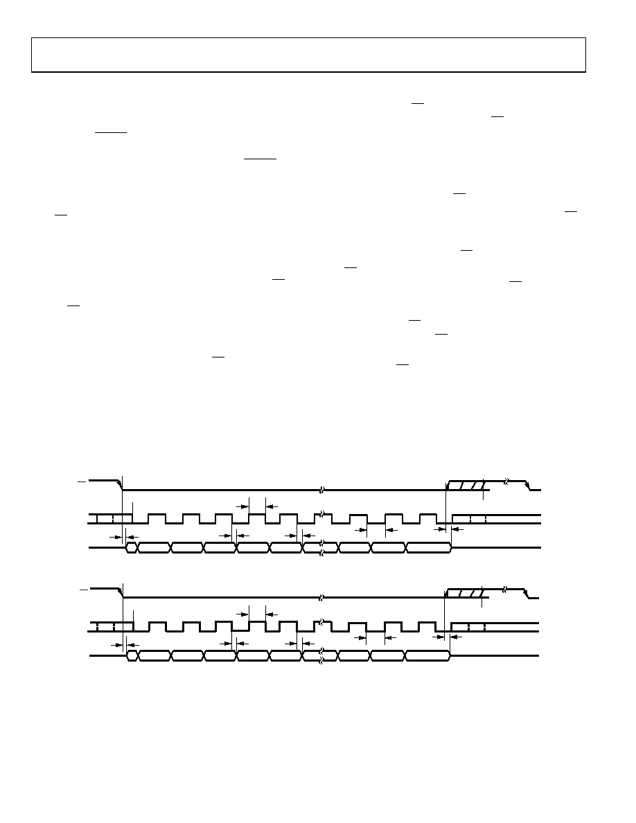
SERIAL INTERFACE
Figure 25 and Figure 26 show the detailed timing diagram for
serial interfacing to the AD7366 and the AD7367. On the
falling edge of CNVST, the AD7366/AD7367 simultaneously
convert the selected channels. These conversions are performed
using the on-chip oscillator. After the falling edge of CNVST,
the BUSY signal goes high, indicating that the conversion has
started. The BUSY signal returns low when the conversion has
been completed. The data can now be read from the
DOUT pins.
The CS and SCLK signals are required to transfer data from the
AD7366/AD7367. The AD7366/AD7367 have two output pins
corresponding to each ADC. Data can be read from the AD7366/
AD7367 using both DOUTA and DOUTB. Alternatively, a single
output pin of the user’s choice can be used. The SCLK input
signal provides the clock source for the serial interface. The CS
goes low to access data from the AD7366/AD7367. The falling
edge of CS takes the bus out of three-state and clocks out the
MSB of the conversion result. The data stream consists of
12 bits of data for the AD7366 and 14 bits of data for the
AD7367, MSB first. The first bit of the conversion result is
valid on the first SCLK falling edge after the CS falling edge.
The subsequent 11/13 bits of data for the AD7366/AD7367,
respectively, are clocked out on the falling edge of the SCLK
signal. A minimum of 12 clock pulses must be provided to the
AD7366 to access each conversion result, and a minimum of
14 clock pulses must be provided to the AD7367 to access the
conversion result. Figure 25 shows how a 12 SCLK read is used
to access the conversion results for the AD7366, and Figure 26
illustrates the case for the AD7367 with a 14 SCLK read.
On the rising edge of CS the conversion is terminated and
DOUTA and DOUTB return to three-state. If CS is not brought
high, but is instead held low for an additional 14 SCLK cycles
the data from the other DOUT pin follows on the selected
DOUT pin. Note, the second serial result from the AD7366 is
preceeded by two zeros. See Figure 27 and Figure 28, where
DOUTA is shown. In this case, the DOUT line in use returns to
three-state on the rising edge of CS.
If the falling edge of SCLK coincides with the falling edge of CS,
the falling edge of SCLK is not acknowledged by the AD7366/
AD7367, and the next falling edge of SCLK is the first one
registered after the falling edge of CS.
The CS pin can be brought low before the BUSY signal goes
low, indicating the end of a conversion. When CS is at a logic
low state, the data bus is brought out of three-state. This feature
can be used to ensure that the MSB is valid on the falling edge
of BUSY by bringing CS low a minimum of t4 before the BUSY
signal goes low. The dotted CS
illustrates this feature.
Alternatively, the CS pin can be tied to a low logic state continu-
ously. In this case, the DOUT pins never enter three-state and the
data bus is continuously active. Under these conditions, the MSB
of the conversion result for the AD7366/AD7367 is available on
the falling edge of the BUSY signal. The next most significant
bit is available on the first SCLK falling edge after the BUSY
signal has gone low. This mode of operation enables the user to
read the MSB as soon as it is made available by the converter.
DOUTA
DOUTB
THREE-
STATE
THREE-STATE
CS
SCLK
1
5
12
2
3
4
DB10
DB11
DB9
DB8
DB2
DB1
DB0
t5
t6
t8
t4
t7
t9
06703-
027
Figure 25. Serial Interface Timing Diagram for the AD7366
DOUTA
DOUTB THREE-
STATE
THREE-STATE
CS
SCLK
1
5
14
2
3
4
DB12
DB13
DB11
DB10
DB2
DB1
DB0
t5
t6
t8
t4
t7
t9
06703-
028
Figure 26. Serial Interface Timing Diagram for the AD7367
相关PDF资料 |
PDF描述 |
|---|---|
| EBC15DRTS-S734 | CONN EDGECARD 30POS DIP .100 SLD |
| EBC43DCMD | CONN EDGECARD 86POS .100 WW |
| ESC06DRTN-S734 | CONN EDGECARD 12POS DIP .100 SLD |
| EVAL-AD7328SDZ | BOARD EVAL FOR AD7328 |
| ESC06DRTH-S734 | CONN EDGECARD 12POS DIP .100 SLD |
相关代理商/技术参数 |
参数描述 |
|---|---|
| EVAL-AD7367CBZ | 制造商:AD 制造商全称:Analog Devices 功能描述:True Bipolar Input, Dual 1 レs, 12-/14-Bit, 2-Channel SAR ADCs |
| EVAL-AD7367SDZ | 功能描述:数据转换 IC 开发工具 EVALUATION CONTROL BOARD I.C. RoHS:否 制造商:Texas Instruments 产品:Demonstration Kits 类型:ADC 工具用于评估:ADS130E08 接口类型:SPI 工作电源电压:- 6 V to + 6 V |
| EVAL-AD7376EBZ | 功能描述:BOARD EVAL FOR AD7376 RoHS:是 类别:编程器,开发系统 >> 评估演示板和套件 系列:- 标准包装:1 系列:- 主要目的:电信,线路接口单元(LIU) 嵌入式:- 已用 IC / 零件:IDT82V2081 主要属性:T1/J1/E1 LIU 次要属性:- 已供物品:板,电源,线缆,CD 其它名称:82EBV2081 |
| EVAL-AD7400AEBZ | 制造商:Analog Devices 功能描述:EVALUATION BOARD I.C. - Bulk |
| EVAL-AD7400AEDZ | 功能描述:BOARD EVAL AD7400A RoHS:是 类别:编程器,开发系统 >> 评估板 - 模数转换器 (ADC) 系列:iCoupler® 产品培训模块:Obsolescence Mitigation Program 标准包装:1 系列:- ADC 的数量:1 位数:12 采样率(每秒):94.4k 数据接口:USB 输入范围:±VREF/2 在以下条件下的电源(标准):- 工作温度:-40°C ~ 85°C 已用 IC / 零件:MAX11645 已供物品:板,软件 |
发布紧急采购,3分钟左右您将得到回复。