- 您现在的位置:买卖IC网 > PDF目录17050 > EVAL-AD7401AEDZ (Analog Devices Inc)BOARD EVAL FOR AD7401 PDF资料下载
参数资料
| 型号: | EVAL-AD7401AEDZ |
| 厂商: | Analog Devices Inc |
| 文件页数: | 7/20页 |
| 文件大小: | 0K |
| 描述: | BOARD EVAL FOR AD7401 |
| 标准包装: | 1 |
| 系列: | iCoupler® |
| ADC 的数量: | 1 |
| 位数: | 16 |
| 采样率(每秒): | 20M |
| 数据接口: | 串行 |
| 输入范围: | ±320 mV |
| 在以下条件下的电源(标准): | 105mW @ 20MSPS |
| 工作温度: | -40°C ~ 125°C |
| 已用 IC / 零件: | AD7401A |
| 已供物品: | 板 |

AD7401A
Rev. C | Page 15 of 20
DIFFERENTIAL INPUTS
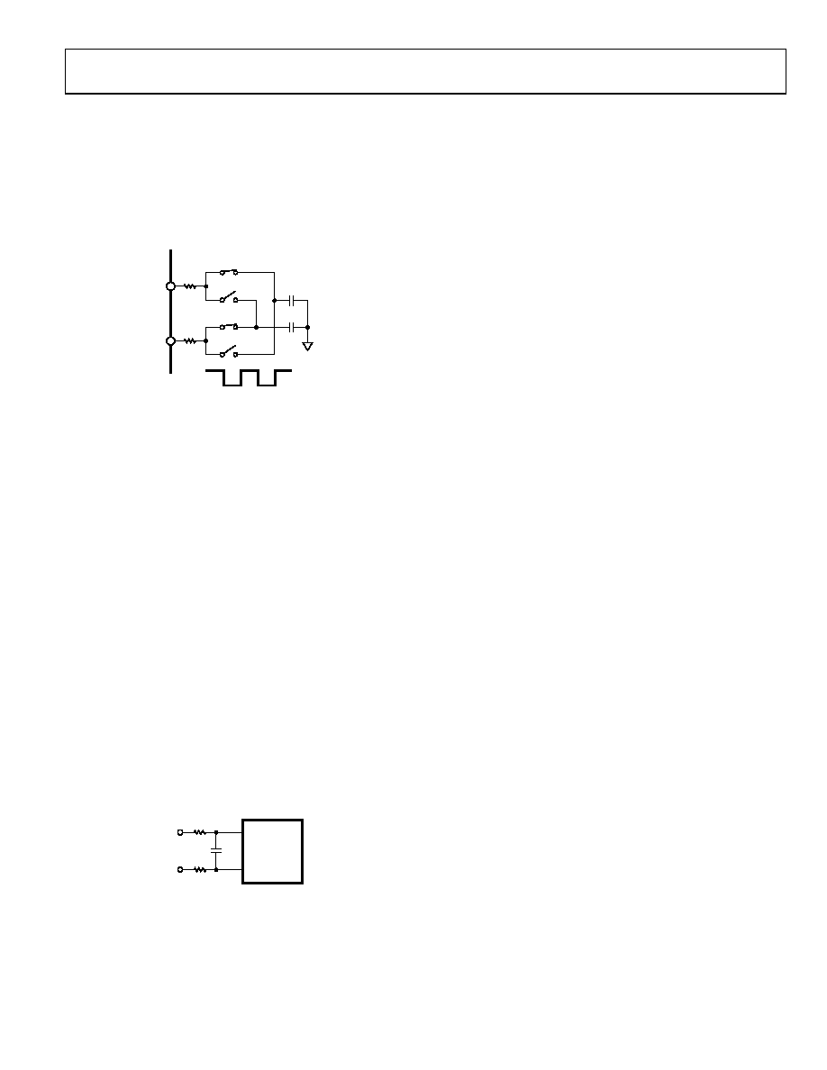
The analog input to the modulator is a switched capacitor
design. The analog signal is converted into charge by highly
linear sampling capacitors. A simplified equivalent circuit
diagram of the analog input is shown in Figure 24. A signal
source driving the analog input must be able to provide the
charge onto the sampling capacitors every half MCLKIN cycle
and settle to the required accuracy within the next half cycle.
φA
φB
1k
VIN–
φA
φB
1k
VIN+
2pF
φA
MCLKIN
0
73
32
-0
24
Figure 24. Analog Input Equivalent Circuit
Because the AD7401A samples the differential voltage across
its analog inputs, low noise performance is attained with an
input circuit that provides low common-mode noise at each
input. The amplifiers used to drive the analog inputs play a
critical role in attaining the high performance available from the
AD7401A.
When a capacitive load is switched onto the output of an op
amp, the amplitude momentarily drops. The op amp tries to
correct the situation and, in the process, hits its slew rate limit.
This nonlinear response, which can cause excessive ringing,
can lead to distortion. To remedy the situation, a low-pass RC
filter can be connected between the amplifier and the input
to the AD7401A. The external capacitor at each input aids
in supplying the current spikes created during the sampling
process, and the resistor isolates the op amp from the transient
nature of the load.
The recommended circuit configuration for driving the
differential inputs to achieve best performance is shown in
Figure 25. A capacitor between the two input pins sources or
sinks charge to allow most of the charge that is needed by one
input to be effectively supplied by the other input. The series
resistor again isolates any op amp from the current spikes
created during the sampling process. Recommended values for
the resistors and capacitor are 22 Ω and 47 pF, respectively.
R
VIN–
R
VIN+
C
AD7401A
07
33
2-
02
5
Figure 25. Differential Input RC Network
CURRENT SENSING APPLICATIONS
The AD7401A is ideally suited for current sensing applications
where the voltage across a shunt resistor is monitored. The load
current flowing through an external shunt resistor produces a
voltage at the input terminals of the AD7401A. The AD7401A
provides isolation between the analog input from the current
sensing resistor and the digital outputs. By selecting the appro-
priate shunt resistor value, a variety of current ranges can be
monitored.
Choosing RSHUNT
The shunt resistor values used in conjunction with the AD7401A
are determined by the specific application requirements in
terms of voltage, current, and power. Small resistors minimize
power dissipation, while low inductance resistors prevent any
induced voltage spikes, and good tolerance devices reduce
current variations. The final values chosen are a compromise
between low power dissipation and good accuracy. Low value
resistors have less power dissipated in them, but higher value
resistors may be required to utilize the full input range of the
ADC, thus achieving maximum SNR performance.
When the peak sense current is known, the voltage range of the
AD7401A (±200 mV) is divided by the maximum sense current
to yield a suitable shunt value. If the power dissipation in the
shunt resistor is too large, the shunt resistor can be reduced
and less of the ADC input range is used. Using less of the ADC
input range results in performance that is more susceptible to
noise and offset errors because offset errors are fixed and are
thus more significant when smaller input ranges are used.
RSHUNT must be able to dissipate the I2R power losses. If the
power dissipation rating of the resistor is exceeded, its value
may drift or the resistor may be damaged, resulting in an open
circuit. This can result in a differential voltage across the ter-
minals of the AD401A in excess of the absolute maximum
ratings. If ISENSE has a large high frequency component, take
care to choose a resistor with low inductance.
VOLTAGE SENSING APPLICATIONS
The AD7401A can also be used for isolated voltage monitoring.
For example, in motor control applications, it can be used to
sense bus voltage. In applications where the voltage being moni-
tored exceeds the specified analog input range of the AD7401A,
a voltage divider network can be used to reduce the voltage to
be monitored to the required range.
相关PDF资料 |
PDF描述 |
|---|---|
| HI5860SOICEVAL1 | EVALUATION PLATFORM SOIC HI5860 |
| REC5-0505DRW/H2/A | CONV DC/DC 5W 4.5-9VIN +/-05VOUT |
| REC5-483.3DRW/H2/C | CONV DC/DC 5W 36-72VIN +/-3.3V |
| GCM22DCMH | CONN EDGECARD 44POS .156 WW |
| ISL5961EVAL1 | ISL5961 -SOICEVALUATION PLATF |
相关代理商/技术参数 |
参数描述 |
|---|---|
| EVAL-AD7401EB | 制造商:AD 制造商全称:Analog Devices 功能描述:Isolated Sigma-Delta Modulator |
| EVAL-AD7401EDZ | 功能描述:BOARD EVALUATION FOR AD7401 RoHS:是 类别:编程器,开发系统 >> 评估板 - 模数转换器 (ADC) 系列:iCoupler® 产品培训模块:Obsolescence Mitigation Program 标准包装:1 系列:- ADC 的数量:1 位数:12 采样率(每秒):94.4k 数据接口:USB 输入范围:±VREF/2 在以下条件下的电源(标准):- 工作温度:-40°C ~ 85°C 已用 IC / 零件:MAX11645 已供物品:板,软件 |
| EVAL-AD74111EBZ | 功能描述:BOARD EVAL FOR AD74111 RoHS:是 类别:编程器,开发系统 >> 评估演示板和套件 系列:- 标准包装:1 系列:PSoC® 主要目的:电源管理,热管理 嵌入式:- 已用 IC / 零件:- 主要属性:- 次要属性:- 已供物品:板,CD,电源 |
| EVAL-AD74122EB-U1 | 制造商:Analog Devices 功能描述:- Bulk |
| EVAL-AD7414/15EB | 制造商:AD 制造商全称:Analog Devices 功能描述:【0.5C Accurate, 10-Bit Digital Temperature Sensors in SOT-23 |
发布紧急采购,3分钟左右您将得到回复。