- 您现在的位置:买卖IC网 > PDF目录17038 > EVAL-AD7610CBZ (Analog Devices Inc)BOARD EVALUATION FOR AD7610 PDF资料下载
参数资料
| 型号: | EVAL-AD7610CBZ |
| 厂商: | Analog Devices Inc |
| 文件页数: | 14/32页 |
| 文件大小: | 0K |
| 描述: | BOARD EVALUATION FOR AD7610 |
| 标准包装: | 1 |
| 系列: | PulSAR® |
| ADC 的数量: | 1 |
| 位数: | 16 |
| 采样率(每秒): | 250k |
| 数据接口: | 串行,并联 |
| 在以下条件下的电源(标准): | 90mW @ 250kSPS |
| 工作温度: | -40°C ~ 85°C |
| 已用 IC / 零件: | AD7610 |
| 已供物品: | 板 |
第1页第2页第3页第4页第5页第6页第7页第8页第9页第10页第11页第12页第13页当前第14页第15页第16页第17页第18页第19页第20页第21页第22页第23页第24页第25页第26页第27页第28页第29页第30页第31页第32页
Data Sheet
AD7610
Rev. A | Page 21 of 32
Internal Reference (REF = 5 V)
(PDREF = Low, PDBUF = Low)
To use the internal reference, the PDREF and PDBUF inputs
must be low. This enables the on-chip band gap reference, buffer,
and TEMP sensor resulting in a 5.00 V reference on the REF pin.
The internal reference is temperature-compensated to 5.000 V
±35 mV. The reference is trimmed to provide a typical drift of
3 ppm/°C. This typical drift characteristic is shown in Figure 19.
External 2.5 V Reference and Internal Buffer (REF = 5 V)
(PDREF = High, PDBUF = Low)
To use an external reference with the internal buffer, PDREF
should be high and PDBUF should be low. This powers down
the internal reference and allows the 2.5 V reference to be applied
to REFBUFIN producing 5 V on the REF pin. The internal ref-
erence buffer is useful in multiconverter applications since a
buffer is typically required in these applications.
External 5 V Reference (PDREF = High, PDBUF = High)
To use an external reference directly on the REF pin, PDREF
and PDBUF should both be high. PDREF and PDBUF power
down the internal reference and the internal reference buffer,
respectively. For improved drift performance, an external ref-
erence such as the ADR445 or ADR435 is recommended.
Reference Decoupling
Whether using an internal or external reference, the AD7610
voltage reference input (REF) has a dynamic input impedance;
therefore, it should be driven by a low impedance source with
efficient decoupling between the REF and REFGND inputs. This
decoupling depends on the choice of the voltage reference, but
usually consists of a low ESR capacitor connected to REF and
REFGND with minimum parasitic inductance. A 22 μF (X5R,
1206 size) ceramic chip capacitor (or 47 μF tantalum capacitor)
is appropriate when using either the internal reference or the
ADR445/ADR435 external reference.
The placement of the reference decoupling is also important to
the performance of the AD7610. The decoupling capacitor should
be mounted on the same side as the ADC right at the REF pin
with a thick PCB trace. The REFGND should also connect to
the reference decoupling capacitor with the shortest distance
and to the analog ground plane with several vias.
For applications that use multiple AD7610 or other PulSAR
devices, it is more effective to use the internal reference buffer
to buffer the external 2.5 V reference voltage.
The voltage reference temperature coefficient (TC) directly
impacts full scale; therefore, in applications where full-scale
accuracy matters, care must be taken with the TC. For instance, a
±15 ppm/°C TC of the reference changes full-scale by ±1 LSB/°C.
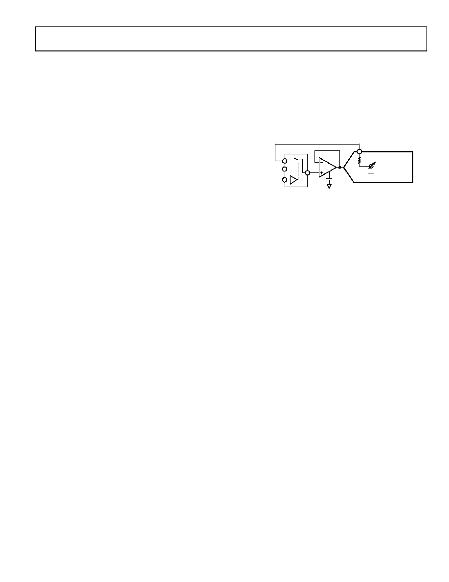
Temperature Sensor
When the internal reference is enabled (PDREF = PDBUF =
low), the on-chip temperature sensor output (TEMP) is enabled
and can be use to measure the temperature of the AD7610. To
improve the calibration accuracy over the temperature range, the
output of the TEMP pin is applied to one of the inputs of the
analog switch (such as ADG779), and the ADC itself is used to
measure its own temperature. This configuration is shown in
ADG779
CC
ANALOG INPUT
AD7610
IN+
TEMPERATURE
SENSOR
TEMP
06
39
5-
03
0
Figure 30. Use of the Temperature Sensor
POWER SUPPLIES
The AD7610 uses five sets of power supply pins:
AVDD: analog 5 V core supply
VCC: analog high voltage positive supply
VEE: high voltage negative supply
DVDD: digital 5 V core supply
OVDD: digital input/output interface supply
Core Supplies
The AVDD and DVDD supply the AD7610 analog and digital
cores respectively. Sufficient decoupling of these supplies is
required consisting of at least a 10 μF capacitor and 100 nF on
each supply. The 100 nF capacitors should be placed as close as
possible to the AD7610. To reduce the number of supplies needed,
the DVDD can be supplied through a simple RC filter from the
analog supply, as shown in Figure 27.
High Voltage Supplies
The high voltage bipolar supplies, VCC and VEE are required
and must be at least 2 V larger than the maximum input, VIN.
For example, if using the bipolar 10 V range, the supplies should
be ±12 V minimum. Sufficient decoupling of these supplies is
also required consisting of at least a 10 μF capacitor and 100 nF
on each supply. For unipolar operation, the VEE supply can be
grounded with some slight THD performance degradation.
Digital Output Supply
The OVDD supplies the digital outputs and allows direct interface
with any logic working between 2.3 V and 5.25 V. OVDD should
be set to the same level as the system interface. Sufficient decou-
pling is required consisting of at least a 10 μF capacitor and 100 nF
with the 100 nF placed as close as possible to the AD7610.
相关PDF资料 |
PDF描述 |
|---|---|
| EVAL-AD7651CBZ | BOARD EVALUATION FOR AD7651 |
| EVAL-AD7694CBZ | BOARD EVALUATION FOR AD7694 |
| 0210490994 | CABLE JUMPER 1.25MM .127M 29POS |
| RBC08DREH-S93 | CONN EDGECARD 16POS .100 EYELET |
| EVAL-AD7684CBZ | BOARD EVALUATION FOR AD7684 |
相关代理商/技术参数 |
参数描述 |
|---|---|
| EVAL-AD7610EDZ | 功能描述:BOARD EVAL FOR AD7610 RoHS:是 类别:编程器,开发系统 >> 评估板 - 模数转换器 (ADC) 系列:* 产品培训模块:Obsolescence Mitigation Program 标准包装:1 系列:- ADC 的数量:1 位数:12 采样率(每秒):94.4k 数据接口:USB 输入范围:±VREF/2 在以下条件下的电源(标准):- 工作温度:-40°C ~ 85°C 已用 IC / 零件:MAX11645 已供物品:板,软件 |
| EVAL-AD7612CB | 制造商:Analog Devices 功能描述:EVAL BD FOR AD7612 - Bulk |
| EVAL-AD7612CBZ | 功能描述:BOARD EVALUATION FOR AD7612 RoHS:是 类别:编程器,开发系统 >> 评估板 - 模数转换器 (ADC) 系列:PulSAR® 产品培训模块:Obsolescence Mitigation Program 标准包装:1 系列:- ADC 的数量:1 位数:12 采样率(每秒):94.4k 数据接口:USB 输入范围:±VREF/2 在以下条件下的电源(标准):- 工作温度:-40°C ~ 85°C 已用 IC / 零件:MAX11645 已供物品:板,软件 |
| EVAL-AD7612EDZ | 功能描述:BOARD EVAL FOR AD7612 RoHS:是 类别:编程器,开发系统 >> 评估板 - 模数转换器 (ADC) 系列:PulSAR® 产品培训模块:Obsolescence Mitigation Program 标准包装:1 系列:- ADC 的数量:1 位数:12 采样率(每秒):94.4k 数据接口:USB 输入范围:±VREF/2 在以下条件下的电源(标准):- 工作温度:-40°C ~ 85°C 已用 IC / 零件:MAX11645 已供物品:板,软件 |
| EVAL-AD7621CB2 | 制造商:AD 制造商全称:Analog Devices 功能描述:16-Bit, 2 LSB INL, 3 MSPS PulSAR?? ADC |
发布紧急采购,3分钟左右您将得到回复。