- 您现在的位置:买卖IC网 > PDF目录17039 > EVAL-AD7622CBZ (Analog Devices Inc)BOARD EVALUATION FOR AD7622 PDF资料下载
参数资料
| 型号: | EVAL-AD7622CBZ |
| 厂商: | Analog Devices Inc |
| 文件页数: | 9/28页 |
| 文件大小: | 0K |
| 描述: | BOARD EVALUATION FOR AD7622 |
| 标准包装: | 1 |
| 系列: | PulSAR® |
| ADC 的数量: | 1 |
| 位数: | 16 |
| 采样率(每秒): | 2M |
| 数据接口: | 串行,并联 |
| 输入范围: | ±VREF |
| 在以下条件下的电源(标准): | 70mW @ 2MSPS |
| 工作温度: | -40°C ~ 85°C |
| 已用 IC / 零件: | AD7622 |
| 已供物品: | 板 |
| 相关产品: | AD7622BSTZ-ND - IC ADC 16BIT DIFFERENTIAL 48LQFP AD7622BCPZ-ND - IC ADC 16BIT DIFFERENTL 48-LFCSP AD7622BSTZRL-ND - IC ADC 16BIT DIFFERENTL 48-LQFP AD7622BCPZRL-ND - IC ADC 16BIT DIFFERENTL 48-LFCSP |
第1页第2页第3页第4页第5页第6页第7页第8页当前第9页第10页第11页第12页第13页第14页第15页第16页第17页第18页第19页第20页第21页第22页第23页第24页第25页第26页第27页第28页
AD7622
Rev. 0 | Page 17 of 28
TYPICAL CONNECTION DIAGRAM
Figure 24 shows a typical connection diagram for the AD7622.
Different circuitry shown in this diagram is optional and is
discussed in the following sections.
ANALOG INPUTS
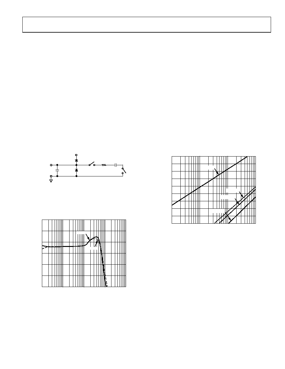
Figure 25 shows an equivalent circuit of the input structure of
the AD7622.
The two diodes, D1 and D2, provide ESD protection for the
analog inputs IN+ and IN. Care must be taken to ensure that
the analog input signal never exceeds the supply rails by more
than 0.3 V, because this causes the diodes to become forward-
biased and to start conducting current. These diodes can handle
a forward-biased current of 100 mA maximum. For instance,
these conditions could eventually occur when the input buffer’s
U1 or U2 supplies are different from AVDD. In such a case, an
input buffer with a short-circuit current limitation can be used
to protect the part.
D1
RIN
CIN
D2
IN+ OR IN–
AGND
AVDD
CPIN
06
02
3-
02
4
Figure 25. AD7622 Simplified Analog Input
The analog input of the AD7622 is a true differential structure.
By using this differential input, small signals common to both
inputs are rejected, as shown in Figure 26, representing the
typical CMRR over frequency with internal and external references.
75
45
1
10000
FREQUENCY (kHz)
CM
R
(
d
B)
10
100
1000
50
55
60
65
70
06
02
3-
02
5
INT REF
EXT REF
Figure 26. Analog Input CMRR vs. Frequency
During the acquisition phase for ac signals, the impedance of
the analog inputs, IN+ and IN, can be modeled as a parallel
combination of capacitor CPIN and the network formed by the
series connection of RIN and CIN. CPIN is primarily the pin
capacitance. RIN is typically 175 Ω and is a lumped component
comprised of some serial resistors and the on resistance of the
switches. CIN is typically 12 pF and is mainly the ADC sampling
capacitor. During the conversion phase, when the switches are
opened, the input impedance is limited to CPIN. RIN and CIN
make a 1-pole, low-pass filter that has a typical 3 dB cutoff
frequency of 50 MHz, thereby reducing an undesirable aliasing
effect and limiting the noise coming from the inputs.
Because the input impedance of the AD7622 is very high, the
AD7622 can be directly driven by a low impedance source
without gain error. To further improve the noise filtering achieved
by the AD7622’s analog input circuit, an external 1-pole RC
filter between the amplifier’s outputs and the ADC analog
inputs can be used, as shown in Figure 24. However, large source
impedances significantly affect the ac performance, especially
the total harmonic distortion (THD). The maximum source
impedance depends on the amount of THD that can be
tolerated. The THD degrades as a function of the source
impedance and the maximum input frequency, as shown in
–60
–105
1
1000
T
HD
(
d
B)
10
100
–95
–85
–75
–65
–100
–90
–80
–70
06
02
3-
0
26
INPUT FREQUENCY (kHz)
RS = 500
RS = 100
RS = 50
RS = 15
Figure 27. THD vs. Analog Input Frequency and Source Resistance
MULTIPLEXED INPUTS
When using the full 2 MSPS throughput in multiplexed
applications for a full-scale step, the RC filter, as shown in
These values are chosen to optimize the best SNR performance
of the AD7622. To use the full 2 MSPS throughput in multiplexed
applications, the RC should be adjusted to satisfy t8 (which is
~ 7 × RC time constant). However, lowering R and C increases
the RC filter bandwidth and allows more noise into the AD7622,
which degrades SNR. To preserve the SNR performance in these
applications using the RC filter shown in Figure 24, the AD7622
should be run with t8 > 280 ns; or approximately 1/(t7 + t8) ~
1.55 MSPS in wideband and warp modes.
相关PDF资料 |
PDF描述 |
|---|---|
| RBC08DREN-S93 | CONN EDGECARD 16POS .100 EYELET |
| RSC05DREH-S93 | CONN EDGECARD 10POS .100 EYELET |
| 0210490995 | CABLE JUMPER 1.25MM .127M 29POS |
| RMC05DREH-S93 | CONN EDGECARD 10POS .100 EYELET |
| MLG1005SR20J | INDUCTOR MULTILAYER .20UH 0402 |
相关代理商/技术参数 |
参数描述 |
|---|---|
| EVAL-AD7622EDZ | 功能描述:BOARD EVAL FOR AD7622 RoHS:是 类别:编程器,开发系统 >> 评估板 - 模数转换器 (ADC) 系列:* 产品培训模块:Obsolescence Mitigation Program 标准包装:1 系列:- ADC 的数量:1 位数:12 采样率(每秒):94.4k 数据接口:USB 输入范围:±VREF/2 在以下条件下的电源(标准):- 工作温度:-40°C ~ 85°C 已用 IC / 零件:MAX11645 已供物品:板,软件 |
| EVAL-AD7623CB | 制造商:Analog Devices 功能描述:EVAL KIT FOR 16BIT, 1.33 MSPS PULSAR ADC - Trays |
| EVAL-AD7623CBZ | 功能描述:BOARD EVALUATION FOR AD7623 RoHS:是 类别:编程器,开发系统 >> 评估板 - 模数转换器 (ADC) 系列:PulSAR® 产品培训模块:Obsolescence Mitigation Program 标准包装:1 系列:- ADC 的数量:1 位数:12 采样率(每秒):94.4k 数据接口:USB 输入范围:±VREF/2 在以下条件下的电源(标准):- 工作温度:-40°C ~ 85°C 已用 IC / 零件:MAX11645 已供物品:板,软件 |
| EVAL-AD7623EDZ | 功能描述:BOARD EVAL FOR AD7623 RoHS:是 类别:编程器,开发系统 >> 评估板 - 模数转换器 (ADC) 系列:* 产品培训模块:Obsolescence Mitigation Program 标准包装:1 系列:- ADC 的数量:1 位数:12 采样率(每秒):94.4k 数据接口:USB 输入范围:±VREF/2 在以下条件下的电源(标准):- 工作温度:-40°C ~ 85°C 已用 IC / 零件:MAX11645 已供物品:板,软件 |
| EVAL-AD7625EDZ | 功能描述:数据转换 IC 开发工具 Eval Board 16-BIT 5MSPS ADC I.C RoHS:否 制造商:Texas Instruments 产品:Demonstration Kits 类型:ADC 工具用于评估:ADS130E08 接口类型:SPI 工作电源电压:- 6 V to + 6 V |
发布紧急采购,3分钟左右您将得到回复。