- 您现在的位置:买卖IC网 > PDF目录16993 > EVAL-AD7663CBZ (Analog Devices Inc)BOARD EVALUATION FOR AD7663 PDF资料下载
参数资料
| 型号: | EVAL-AD7663CBZ |
| 厂商: | Analog Devices Inc |
| 文件页数: | 13/24页 |
| 文件大小: | 0K |
| 描述: | BOARD EVALUATION FOR AD7663 |
| 标准包装: | 1 |
| 系列: | PulSAR® |
| ADC 的数量: | 1 |
| 位数: | 16 |
| 采样率(每秒): | 250k |
| 数据接口: | 串行,并联 |
| 输入范围: | ±4 REF |
| 在以下条件下的电源(标准): | 35mW @ 250kSPS |
| 工作温度: | -40°C ~ 85°C |
| 已用 IC / 零件: | AD7663 |
| 已供物品: | 板,CD |
| 相关产品: | AD7663ACPZ-ND - IC ADC 16BIT CMOS 5V 48LFCSP AD7663ACPZRL-ND - IC ADC 16BIT CMOS 5V 48LFCSP AD7663ASTZRL-ND - IC ADC 16BIT CMOS 48-LQFP T/R AD7663ASTZ-ND - IC ADC 16BIT CMOS 48-LQFP |
REV. B
AD7663
–20–
CNVST
SDOUT
SCLK
D1
D0
X
D15
D14
D13
12
3
14
15
16
t3
t35
t36 t37
t31
t32
t16
BUSY
INVSCLK = 0
CS
EXT/
INT = 1
RD = 0
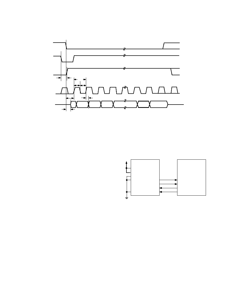
Figure 21. Slave Serial Data Timing for Reading (Read Previous Conversion during Convert)
External Clock Data Read during Conversion
Figure 21 shows the detailed timing diagrams of this method.
During a conversion, while both
CS and RD are LOW, the result
of the previous conversion can be read. The data is shifted out
MSB first with 16 clock pulses, and is valid on both the rising and
the falling edge of the clock. The 16 bits have to be read before
the current conversion is complete. If that is not done, RDERROR
is pulsed HIGH and can be used to interrupt the host interface
to prevent an incomplete data reading. There is no daisy-chain
feature in this mode, and RDC/SDIN input should always be
tied either HIGH or LOW.
To reduce performance degradation due to digital activity, a
fast discontinuous clock of at least 25 MHz is recommended to
ensure that all the bits are read during the first half of the conver-
sion phase.
MICROPROCESSOR INTERFACING
The AD7663 is ideally suited for traditional dc measurement
applications supporting a microprocessor and ac signal processing
applications interfacing to a digital signal processor. The
AD7663 is designed to interface with either a parallel 8-bit or
16-bit wide interface or with a general-purpose Serial Port or I/O
Ports on a microcontroller. A variety of external buffers can be
used with the AD7663 to prevent digital noise from coupling into
the ADC. The following sections illustrate the use of the AD7663
with an SPI equipped microcontroller, the ADSP-21065L and
ADSP-218x signal processors.
SPI Interface (MC68HC11)
Figure 22 shows an interface diagram between the AD7663 and an
SPI-equipped microcontroller, such as the MC68HC11. To
accommodate the slower speed of the microcontroller, the AD7663
acts as a slave device and data must be read after conversion. This
mode also allows the daisy-chain feature. The convert command
could be initiated in response to an internal timer interrupt. The
reading of output data, one byte at a time if necessary, could be
initiated in response to the end-of-conversion signal (BUSY going
LOW) using an interrupt line of the microcontroller. The serial
peripheral interface (SPI) on the MC68HC11 is configured for
Master Mode (MSTR) = 1, Clock Polarity Bit (CPOL) = 0, Clock
Phase Bit (CPHA) = 1, and SPI interrupt enable (SPIE) = 1
by writing to the SPI Control Register (SPCR). The IRQ is
configured for edge-sensitive-only operation (IRQE = 1 in
OPTION register).
IRQ
MC68HC11*
CNVST
AD7663*
BUSY
CS
MISO/SDI
SCK
I/O PORT
SDOUT
SCLK
INVSCLK
EXT/
INT
DVDD
*ADDITIONAL PINS OMITTED FOR CLARITY
SER/
PAR
RD
Figure 22. Interfacing the AD7663 to SPI Interface
ADSP-21065L in Master Serial Interface
As shown in Figure 23, the AD7663 can be interfaced to the
ADSP-21065L using the serial interface in Master Mode without
any glue logic required. This mode combines the advantages of
reducing the wire connections and being able to read the data during
or after conversion at maximum speed transfer (DIVSCLK[0:1]
both low.
The AD7663 is configured for the Internal Clock Mode (EXT/
INT
low) and acts therefore as the master device. The convert com-
mand can be generated by an external low jitter oscillator or, as
shown, by a FLAG output of the ADSP-21065L, or by a frame
output TFS of one Serial Port of the ADSP-21065L that can be used
like a timer. The Serial Port on the ADSP-21065L is configured
for external clock (IRFS = 0), rising edge active (CKRE = 1),
external late framed sync signals (IRFS = 0, LAFS = 1,
RFSR = 1), and active HIGH (LRFS = 0). The Serial Port of
the ADSP-21065L is configured by writing to its receive control
register (SRCTL)—see ADSP-2106x SHARC User’s Manual.
相关PDF资料 |
PDF描述 |
|---|---|
| 1025R-18K | COIL .82UH MOLDED UNSHIELDED |
| VE-J7W-EY | CONVERTER MOD DC/DC 5.5V 50W |
| AD9481-PCBZ | BOARD EVAL 8BIT 250MSPS 44-TQFP |
| VI-J44-EY | CONVERTER MOD DC/DC 48V 50W |
| CDB5525 | EVAL BOARD FOR CS5525 |
相关代理商/技术参数 |
参数描述 |
|---|---|
| EVAL-AD7663EDZ | 制造商:Analog Devices 功能描述:CONVERTER - ADC |
| EVAL-AD7664CB | 制造商:Analog Devices 功能描述:Evaluation Kit For 16-Bit, 570 KSP Pulsar Unipolar CMOS ADC |
| EVAL-AD7664CBZ | 功能描述:BOARD EVALUATION FOR AD7664 RoHS:是 类别:编程器,开发系统 >> 评估板 - 模数转换器 (ADC) 系列:PulSAR® 产品培训模块:Obsolescence Mitigation Program 标准包装:1 系列:- ADC 的数量:1 位数:12 采样率(每秒):94.4k 数据接口:USB 输入范围:±VREF/2 在以下条件下的电源(标准):- 工作温度:-40°C ~ 85°C 已用 IC / 零件:MAX11645 已供物品:板,软件 |
| EVAL-AD7665CB | 制造商:AD 制造商全称:Analog Devices 功能描述:Evaluation Board AD766X/AD767X |
| EVAL-AD7665CBZ | 功能描述:BOARD EVALUATION FOR AD7665 RoHS:是 类别:编程器,开发系统 >> 评估板 - 模数转换器 (ADC) 系列:PulSAR® 产品培训模块:Obsolescence Mitigation Program 标准包装:1 系列:- ADC 的数量:1 位数:12 采样率(每秒):94.4k 数据接口:USB 输入范围:±VREF/2 在以下条件下的电源(标准):- 工作温度:-40°C ~ 85°C 已用 IC / 零件:MAX11645 已供物品:板,软件 |
发布紧急采购,3分钟左右您将得到回复。