- 您现在的位置:买卖IC网 > PDF目录16993 > EVAL-AD7663CBZ (Analog Devices Inc)BOARD EVALUATION FOR AD7663 PDF资料下载
参数资料
| 型号: | EVAL-AD7663CBZ |
| 厂商: | Analog Devices Inc |
| 文件页数: | 7/24页 |
| 文件大小: | 0K |
| 描述: | BOARD EVALUATION FOR AD7663 |
| 标准包装: | 1 |
| 系列: | PulSAR® |
| ADC 的数量: | 1 |
| 位数: | 16 |
| 采样率(每秒): | 250k |
| 数据接口: | 串行,并联 |
| 输入范围: | ±4 REF |
| 在以下条件下的电源(标准): | 35mW @ 250kSPS |
| 工作温度: | -40°C ~ 85°C |
| 已用 IC / 零件: | AD7663 |
| 已供物品: | 板,CD |
| 相关产品: | AD7663ACPZ-ND - IC ADC 16BIT CMOS 5V 48LFCSP AD7663ACPZRL-ND - IC ADC 16BIT CMOS 5V 48LFCSP AD7663ASTZRL-ND - IC ADC 16BIT CMOS 48-LQFP T/R AD7663ASTZ-ND - IC ADC 16BIT CMOS 48-LQFP |
REV. B
AD7663
–15–
Voltage Reference Input
The AD7663 uses an external 2.5 V voltage reference.
The voltage reference input REF of the AD7663 has a dynamic
input impedance; it should therefore be driven by a low impedance
source with an efficient decoupling between REF and REFGND
inputs. This decoupling depends on the choice of the voltage
reference but usually consists of a 1 F ceramic capacitor and a
low ESR tantalum capacitor connected to the REF and REFGND
inputs with minimum parasitic inductance. 47 F is an appropriate
value for the tantalum capacitor when used with one of the
recommended reference voltages:
The low noise, low temperature drift ADR421 and AD780
voltage reference
The low power ADR291 voltage reference
The low cost AD1582 voltage reference
For applications using multiple AD7663s, it is more effective to
buffer the reference voltage with a low noise, very stable op amp
like the AD8031.
Care should also be taken with the reference temperature coefficient
of the voltage reference that directly affects the full-scale accu-
racy if this parameter matters. For instance, a ±15 ppm/°C
tempco of the reference changes the full scale by ±1 LSB/°C.
Note that VREF , as mentioned in the Specification tables, could be
increased to AVDD – 1.85 V. The benefit here is the increased
SNR obtained as a result of this increase. Since the input range is
defined in terms of VREF, this would essentially increase the ±REF
range from ±2.5 V to ±3 V and so on with an AVDD above
4.85 V. The theoretical improvement as a result of this increase
in reference is 1.58 dB (20 log [3/2.5]). Due to the theoretical
quantization noise, however, the observed improvement is approxi-
mately 1 dB. The AD780 can be selected with a 3 V reference
voltage.
Scaler Reference Input (Bipolar Input Ranges)
When using the AD7663 with bipolar input ranges, the connection
diagram in Figure 5 shows a reference buffer amplifier. This
buffer amplifier is required to isolate the REF pin from the signal
dependent current in the INx pin. A high speed op amp, such as
the AD8031, can be used with a single 5 V power supply with-
out degrading the performance of the AD7663. The buffer must
have good settling characteristics and provide low total noise
within the input bandwidth of the AD7663.
Power Supply
The AD7663 uses three sets of power supply pins: an analog 5 V
supply AVDD, a digital 5 V core supply DVDD, and a digital
input/output interface supply OVDD. The OVDD supply allows
direct interface with any logic working between 2.7 V and DVDD
+ 0.3 V. To reduce the number of supplies needed, the digital
core (DVDD) can be supplied through a simple RC filter from the
analog supply as shown in Figure 5. The AD7663 is independent
of power supply sequencing, once OVDD does not exceed DVDD
by more than 0.3 V, and thus free from supply voltage induced
latch-up. Additionally, it is very insensitive to power supply
variations over a wide frequency range as shown in Figure 9.
110
105
100
95
90
85
80
75
70
65
60
55
50
1
10
100
1000
PSRR
–
dB
FREQUENCY – kHz
Figure 9. PSRR vs. Frequency
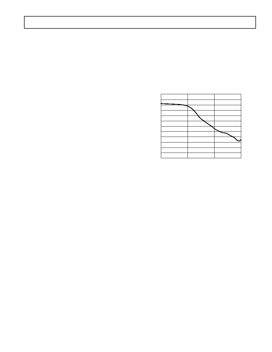
POWER DISSIPATION
The AD7663 automatically reduces its power consumption at
the end of each conversion phase. During the acquisition phase,
the operating currents are very low, which allows a significant
power savings when the conversion rate is reduced as shown in
Figure 10. This feature makes the AD7663 ideal for very low
power battery applications.
This does not take into account the power, if any, dissipated by
the input resistive scaler that depends on the input voltage range
used and the analog input voltage even in power-down mode.
There is no power dissipated when the 0 V to 2.5 V is used or
when both the analog input voltage is 0V and a unipolar range,
0V to 5 V or 0 V to 10 V, is used.
It should be noted that the digital interface remains active even
during the acquisition phase. To reduce the operating digital
supply currents even further, the digital inputs need to be driven
close to the power rails (i.e., DVDD and DGND) and OVDD
should not exceed DVDD by more than 0.3 V.
相关PDF资料 |
PDF描述 |
|---|---|
| 1025R-18K | COIL .82UH MOLDED UNSHIELDED |
| VE-J7W-EY | CONVERTER MOD DC/DC 5.5V 50W |
| AD9481-PCBZ | BOARD EVAL 8BIT 250MSPS 44-TQFP |
| VI-J44-EY | CONVERTER MOD DC/DC 48V 50W |
| CDB5525 | EVAL BOARD FOR CS5525 |
相关代理商/技术参数 |
参数描述 |
|---|---|
| EVAL-AD7663EDZ | 制造商:Analog Devices 功能描述:CONVERTER - ADC |
| EVAL-AD7664CB | 制造商:Analog Devices 功能描述:Evaluation Kit For 16-Bit, 570 KSP Pulsar Unipolar CMOS ADC |
| EVAL-AD7664CBZ | 功能描述:BOARD EVALUATION FOR AD7664 RoHS:是 类别:编程器,开发系统 >> 评估板 - 模数转换器 (ADC) 系列:PulSAR® 产品培训模块:Obsolescence Mitigation Program 标准包装:1 系列:- ADC 的数量:1 位数:12 采样率(每秒):94.4k 数据接口:USB 输入范围:±VREF/2 在以下条件下的电源(标准):- 工作温度:-40°C ~ 85°C 已用 IC / 零件:MAX11645 已供物品:板,软件 |
| EVAL-AD7665CB | 制造商:AD 制造商全称:Analog Devices 功能描述:Evaluation Board AD766X/AD767X |
| EVAL-AD7665CBZ | 功能描述:BOARD EVALUATION FOR AD7665 RoHS:是 类别:编程器,开发系统 >> 评估板 - 模数转换器 (ADC) 系列:PulSAR® 产品培训模块:Obsolescence Mitigation Program 标准包装:1 系列:- ADC 的数量:1 位数:12 采样率(每秒):94.4k 数据接口:USB 输入范围:±VREF/2 在以下条件下的电源(标准):- 工作温度:-40°C ~ 85°C 已用 IC / 零件:MAX11645 已供物品:板,软件 |
发布紧急采购,3分钟左右您将得到回复。