- 您现在的位置:买卖IC网 > PDF目录17031 > EVAL-AD7671CBZ (Analog Devices Inc)BOARD EVALUATION FOR AD7671 PDF资料下载
参数资料
| 型号: | EVAL-AD7671CBZ |
| 厂商: | Analog Devices Inc |
| 文件页数: | 14/24页 |
| 文件大小: | 0K |
| 描述: | BOARD EVALUATION FOR AD7671 |
| 标准包装: | 1 |
| 系列: | PulSAR® |
| ADC 的数量: | 1 |
| 位数: | 16 |
| 采样率(每秒): | 1M |
| 数据接口: | 串行,并联 |
| 输入范围: | ±4 REF |
| 在以下条件下的电源(标准): | 112mW @ 1MSPS |
| 工作温度: | -40°C ~ 85°C |
| 已用 IC / 零件: | AD7671 |
| 已供物品: | 板 |
| 相关产品: | AD7671ACPZ-ND - IC ADC 16BIT CMOS 1MSPS 48LFCSP AD7671ACPZRL-ND - IC ADC 16BIT CMOS 1MSPS 48LFCSP AD7671ASTZRL-ND - IC ADC 16BIT CMOS 1MSPS 48LQFP AD7671ASTZ-ND - IC ADC 16BIT CMOS 1MSPS 48-LQFP |
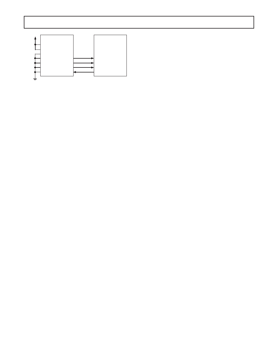
AD7671
–21–
RFS
ADSP-21065L*
SHARC
CNVST
AD7671*
CS
SYNC
RD
DR
RCLK
FLAG OR TFS
SDOUT
SCLK
INVSYNC
INVSCLK
EXT/
INT
RDC/SDIN
SER/
PAR
DVDD
*ADDITIONAL PINS OMITTED FOR CLARITY
Figure 23. Interfacing to the ADSP-21065L Using
the Serial Master Mode
APPLICATION HINTS
Layout
The AD7671 has very good immunity to noise on the power
supplies as can be seen in Figure 9. However, care should still
be taken with regard to grounding layout.
The printed circuit board that houses the AD7671 should be
designed so the analog and digital sections are separated and con-
fined to certain areas of the board. This facilitates the use of ground
planes that can be easily separated. Digital and analog ground
planes should be joined in only one place, preferably underneath
the AD7671, or, at least, as close as possible to the AD7671. If
the AD7671 is in a system where multiple devices require analog-
to-digital ground connections, the connection should still be made at
one point only, a star ground point, which should be established
as close as possible to the AD7671.
It is recommended to avoid running digital lines under the device
as these will couple noise onto the die. The analog ground plane
should be allowed to run under the AD7671 to avoid noise
coupling. Fast switching signals like
CNVST or clocks should
be shielded with digital ground to avoid radiating noise to other
sections of the board and should never run near analog signal
paths. Crossover of digital and analog signals should be avoided.
Traces on different but close layers of the board should run at right
angles to each other. This will reduce the effect of feedthrough
through the board.
The power supply lines to the AD7671 should use as large a trace
as possible to provide low impedance paths and reduce the effect of
glitches on the power supply lines. Good decoupling is also impor-
tant to lower the supplies impedance presented to the AD7671
and to reduce the magnitude of the supply spikes. Decoupling
ceramic capacitors, typically 100 nF, should be placed on all of
the power supply pins power supplies pins AVDD, DVDD, and
OVDD close to, and ideally right up against, these pins and
their corresponding ground pins. Additionally, low ESR 10
mF
capacitors should be located in the vicinity of the ADC to further
reduce low frequency ripple.
The DVDD supply of the AD7671 can be either a separate sup-
ply or come from the analog supply, AVDD, or from the digital
interface supply, OVDD. When the system digital supply is noisy,
or fast switching digital signals are present, it is recommended,
if no separate supply is available, to connect the DVDD digital
supply to the analog supply AVDD through an RC filter as shown
in Figure 5 and to connect the system supply to the interface
digital supply OVDD and the remaining digital circuitry. When
DVDD is powered from the system supply, it is useful to insert
a bead to further reduce high frequency spikes.
The AD7671 has five different ground pins: INGND, REFGND,
AGND, DGND, and OGND. INGND is used to sense the
analog input signal. REFGND senses the reference voltage and
should be a low impedance return to the reference because it carries
pulsed currents. AGND is the ground to which most internal ADC
analog signals are referenced. This ground must be connected
with the least resistance to the analog ground plane. DGND must
be tied to the analog or digital ground plane depending on the
configuration. OGND is connected to the digital system ground.
The layout of the decoupling of the reference voltage is important.
The decoupling capacitor should be close to the ADC and con-
nected with short and large traces to minimize parasitic inductances.
Evaluating the AD7671 Performance
A recommended layout for the AD7671 is outlined in the evalua-
tion board for the AD7671. The evaluation board package includes
a fully assembled and tested evaluation board, documentation,
and software for controlling the board from a PC via the Eval-
Control Board.
REV. C
相关PDF资料 |
PDF描述 |
|---|---|
| 94SVP337X0016F12 | CAP ALUM 330UF 16V 20% SMD |
| EVAL-AD7654CBZ | BOARD EVALUATION FOR AD7654 |
| STD17W-P | WIRE & CABLE MARKERS |
| EVAL-AD7653CBZ | BOARD EVALUATION FOR AD7653 |
| MLG1005S30NJ | INDUCTOR MULTILAYER 30NH 0402 |
相关代理商/技术参数 |
参数描述 |
|---|---|
| EVAL-AD7671EDZ | 功能描述:BOARD EVAL FOR AD7671 RoHS:是 类别:编程器,开发系统 >> 评估板 - 模数转换器 (ADC) 系列:* 产品培训模块:Obsolescence Mitigation Program 标准包装:1 系列:- ADC 的数量:1 位数:12 采样率(每秒):94.4k 数据接口:USB 输入范围:±VREF/2 在以下条件下的电源(标准):- 工作温度:-40°C ~ 85°C 已用 IC / 零件:MAX11645 已供物品:板,软件 |
| EVAL-AD7674CB | 功能描述:BOARD EVAL FOR AD7674 RoHS:否 类别:编程器,开发系统 >> 评估板 - 模数转换器 (ADC) 系列:PulSAR® 产品培训模块:Obsolescence Mitigation Program 标准包装:1 系列:- ADC 的数量:1 位数:12 采样率(每秒):94.4k 数据接口:USB 输入范围:±VREF/2 在以下条件下的电源(标准):- 工作温度:-40°C ~ 85°C 已用 IC / 零件:MAX11645 已供物品:板,软件 |
| EVAL-AD7674CBZ | 功能描述:BOARD EVALUATION FOR AD7674 RoHS:是 类别:编程器,开发系统 >> 评估板 - 模数转换器 (ADC) 系列:PulSAR® 产品培训模块:Obsolescence Mitigation Program 标准包装:1 系列:- ADC 的数量:1 位数:12 采样率(每秒):94.4k 数据接口:USB 输入范围:±VREF/2 在以下条件下的电源(标准):- 工作温度:-40°C ~ 85°C 已用 IC / 零件:MAX11645 已供物品:板,软件 |
| EVAL-AD7674EDZ | 功能描述:BOARD EVAL FOR AD7674 RoHS:是 类别:编程器,开发系统 >> 评估板 - 模数转换器 (ADC) 系列:* 产品培训模块:Obsolescence Mitigation Program 标准包装:1 系列:- ADC 的数量:1 位数:12 采样率(每秒):94.4k 数据接口:USB 输入范围:±VREF/2 在以下条件下的电源(标准):- 工作温度:-40°C ~ 85°C 已用 IC / 零件:MAX11645 已供物品:板,软件 |
| EVAL-AD7675CB | 制造商:AD 制造商全称:Analog Devices 功能描述:Evaluation Board AD766X/AD767X |
发布紧急采购,3分钟左右您将得到回复。