- 您现在的位置:买卖IC网 > PDF目录17031 > EVAL-AD7671CBZ (Analog Devices Inc)BOARD EVALUATION FOR AD7671 PDF资料下载
参数资料
| 型号: | EVAL-AD7671CBZ |
| 厂商: | Analog Devices Inc |
| 文件页数: | 18/24页 |
| 文件大小: | 0K |
| 描述: | BOARD EVALUATION FOR AD7671 |
| 标准包装: | 1 |
| 系列: | PulSAR® |
| ADC 的数量: | 1 |
| 位数: | 16 |
| 采样率(每秒): | 1M |
| 数据接口: | 串行,并联 |
| 输入范围: | ±4 REF |
| 在以下条件下的电源(标准): | 112mW @ 1MSPS |
| 工作温度: | -40°C ~ 85°C |
| 已用 IC / 零件: | AD7671 |
| 已供物品: | 板 |
| 相关产品: | AD7671ACPZ-ND - IC ADC 16BIT CMOS 1MSPS 48LFCSP AD7671ACPZRL-ND - IC ADC 16BIT CMOS 1MSPS 48LFCSP AD7671ASTZRL-ND - IC ADC 16BIT CMOS 1MSPS 48LQFP AD7671ASTZ-ND - IC ADC 16BIT CMOS 1MSPS 48-LQFP |
–3–
AD7671
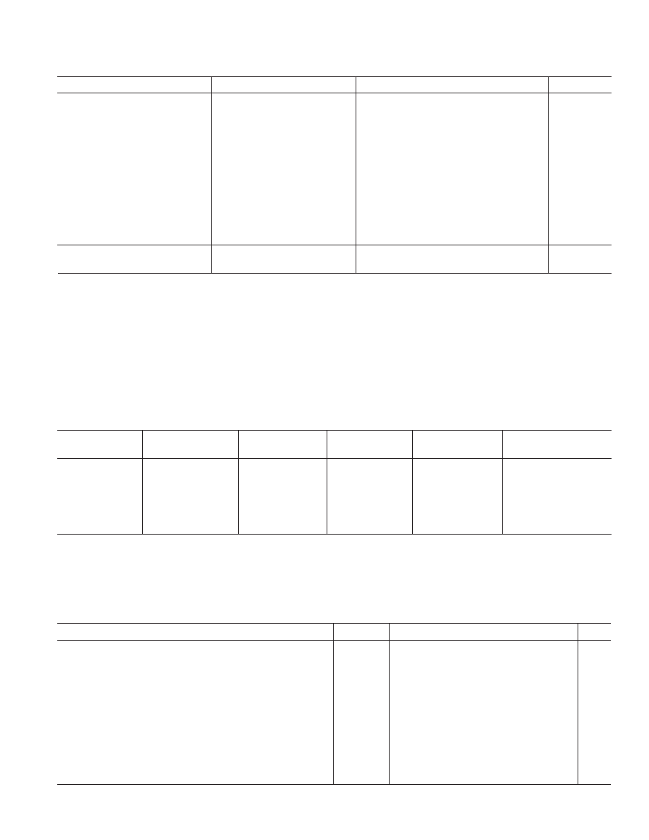
Parameter
Conditions
Min
Typ
Max
Unit
POWER SUPPLIES
Specified Performance
AVDD
4.75
5
5.25
V
DVDD
4.75
5
5.25
V
OVDD
2.7
5.25
4
V
Operating Current
5
1 MSPS Throughput
AVDD
15
mA
DVDD
6
7.2
mA
OVDD
6
37
mA
Power Dissipation
6, 7
666 kSPS Throughput
8
84
95
mW
100 SPS Throughput
8
15
mW
1 MSPS Throughput
5
112
125
mW
In Power-Down Mode
9
7
mW
TEMPERATURE RANGE
10
Specified Performance
TMIN to TMAX
–40
+85
∞C
NOTES
1LSB means least significant bit. With the
±5 V input range, one LSB is 152.588 mV.
2See Definition of Specifications section. These specifications do not include the error contribution from the external reference.
3All specifications in dB are referred to a full-scale input FS. Tested with an input signal at 0.5 dB below full scale, unless otherwise specified.
4The max should be the minimum of 5.25 V and DVDD + 0.3 V.
5In Warp Mode.
6Tested in Parallel Reading Mode.
7Tested with the 0 V to 5 V range and V
IN – VINGND = 0 V. See Power Dissipation section.
8In Impulse Mode.
9With OVDD below DVDD + 0.3 V and all digital inputs forced to DVDD or DGND, respectively.
10Contact factory for extended temperature range.
Specifications subject to change without notice.
Table I. Analog Input Configuration
Input Voltage
Input
Range
IND(4R)
INC(4R)
INB(2R)
INA(R)
Impedance
1
±4 REF2
VIN
INGND
REF
1.63 k
W
±2 REF
VIN
INGND
REF
948
W
±REF
VIN
REF
711
W
0 V to 4 REF
VIN
INGND
948
W
0 V to 2 REF
VIN
INGND
711
W
0 V to REF
VIN
Note 3
NOTES
1Typical analog input impedance.
2With REF = 3 V, in this range, the input should be limited to –11 V to +12 V.
3For this range the input is high impedance.
TIMING SPECIFICATIONS
Parameter
Symbol
Min
Typ
Max
Unit
Refer to Figures 11 and 12
Convert Pulsewidth
t1
5ns
Time between Conversions
t2
1/1.25/1.5
Note 1
ms
(Warp Mode/Normal Mode/Impulse Mode)
CNVST LOW to BUSY HIGH Delay
t3
30
ns
BUSY HIGH All Modes Except in Master Serial Read after
t4
0.75/1/1.25
ms
Convert Mode (Warp Mode/Normal Mode/Impulse Mode)
Aperture Delay
t5
2ns
End of Conversion to BUSY LOW Delay
t6
10
ns
Conversion Time (Warp Mode/Normal Mode/Impulse Mode)
t7
0.75/1/1.25
ms
Acquisition Time
t8
250
ns
RESET Pulsewidth
t9
10
ns
(–40 C to +85 C, AVDD = DVDD = 5 V, OVDD = 2.7 V to 5.25 V, unless otherwise noted.)
REV. C
相关PDF资料 |
PDF描述 |
|---|---|
| 94SVP337X0016F12 | CAP ALUM 330UF 16V 20% SMD |
| EVAL-AD7654CBZ | BOARD EVALUATION FOR AD7654 |
| STD17W-P | WIRE & CABLE MARKERS |
| EVAL-AD7653CBZ | BOARD EVALUATION FOR AD7653 |
| MLG1005S30NJ | INDUCTOR MULTILAYER 30NH 0402 |
相关代理商/技术参数 |
参数描述 |
|---|---|
| EVAL-AD7671EDZ | 功能描述:BOARD EVAL FOR AD7671 RoHS:是 类别:编程器,开发系统 >> 评估板 - 模数转换器 (ADC) 系列:* 产品培训模块:Obsolescence Mitigation Program 标准包装:1 系列:- ADC 的数量:1 位数:12 采样率(每秒):94.4k 数据接口:USB 输入范围:±VREF/2 在以下条件下的电源(标准):- 工作温度:-40°C ~ 85°C 已用 IC / 零件:MAX11645 已供物品:板,软件 |
| EVAL-AD7674CB | 功能描述:BOARD EVAL FOR AD7674 RoHS:否 类别:编程器,开发系统 >> 评估板 - 模数转换器 (ADC) 系列:PulSAR® 产品培训模块:Obsolescence Mitigation Program 标准包装:1 系列:- ADC 的数量:1 位数:12 采样率(每秒):94.4k 数据接口:USB 输入范围:±VREF/2 在以下条件下的电源(标准):- 工作温度:-40°C ~ 85°C 已用 IC / 零件:MAX11645 已供物品:板,软件 |
| EVAL-AD7674CBZ | 功能描述:BOARD EVALUATION FOR AD7674 RoHS:是 类别:编程器,开发系统 >> 评估板 - 模数转换器 (ADC) 系列:PulSAR® 产品培训模块:Obsolescence Mitigation Program 标准包装:1 系列:- ADC 的数量:1 位数:12 采样率(每秒):94.4k 数据接口:USB 输入范围:±VREF/2 在以下条件下的电源(标准):- 工作温度:-40°C ~ 85°C 已用 IC / 零件:MAX11645 已供物品:板,软件 |
| EVAL-AD7674EDZ | 功能描述:BOARD EVAL FOR AD7674 RoHS:是 类别:编程器,开发系统 >> 评估板 - 模数转换器 (ADC) 系列:* 产品培训模块:Obsolescence Mitigation Program 标准包装:1 系列:- ADC 的数量:1 位数:12 采样率(每秒):94.4k 数据接口:USB 输入范围:±VREF/2 在以下条件下的电源(标准):- 工作温度:-40°C ~ 85°C 已用 IC / 零件:MAX11645 已供物品:板,软件 |
| EVAL-AD7675CB | 制造商:AD 制造商全称:Analog Devices 功能描述:Evaluation Board AD766X/AD767X |
发布紧急采购,3分钟左右您将得到回复。