- 您现在的位置:买卖IC网 > PDF目录17039 > EVAL-AD7675CBZ (Analog Devices Inc)BOARD EVALUATION FOR AD7675 PDF资料下载
参数资料
| 型号: | EVAL-AD7675CBZ |
| 厂商: | Analog Devices Inc |
| 文件页数: | 5/20页 |
| 文件大小: | 0K |
| 描述: | BOARD EVALUATION FOR AD7675 |
| 标准包装: | 1 |
| 系列: | PulSAR® |
| ADC 的数量: | 1 |
| 位数: | 16 |
| 采样率(每秒): | 100k |
| 数据接口: | 串行,并联 |
| 输入范围: | ±VREF |
| 在以下条件下的电源(标准): | 17mW @ 100kSPS |
| 工作温度: | -40°C ~ 85°C |
| 已用 IC / 零件: | AD7675 |
| 已供物品: | 板 |
| 相关产品: | AD7675ACPZRL-ND - IC ADC 16BIT SAR 100KSPS 48LFCSP AD7675ACPZ-ND - IC ADC 16BIT SAR 100KSPS 48LFCSP AD7675ASTZ-ND - IC ADC 16BIT DIFF INP 48LQFP AD7675ASTZRL-ND - IC ADC 16BIT DIFF INP 48LQFP |
REV. A
AD7675
–13–
Care should also be taken with the reference temperature coeffi-
cient of the voltage reference which directly affects the full-scale
accuracy if this parameter matters. For instance, a
±15 ppm/°C
tempco of the reference changes the full scale by
±1 LSB/°C.
VREF , as mentioned in the specification table, could be increased
to AVDD – 1.85 V. The benefit here is the increased SNR
obtained as a result of this increase. Since the input range is
defined in terms of VREF, this would essentially increase the
range to make it a
± 3 V input range with an AVDD above
4.85 V. The theoretical improvement as a result of this increase
in reference is 1.58 dB (20 log [3/2.5]). Due to the theoretical
quantization noise, however, the observed improvement is
approximately 1 dB. The AD780 can be selected with a 3 V
reference voltage.
Power Supply
The AD7675 uses three sets of power supply pins: an analog
5V supply AVDD, a digital 5 V core supply DVDD, and a
digital input/output interface supply OVDD. The OVDD
supply allows direct interface with any logic working between
2.7 V and DVDD + 0.3 V. To reduce the number of supplies
needed, the digital core (DVDD) can be supplied through a
simple RC filter from the analog supply as shown in
Figure 5. The AD7675 is independent of power supply
sequencing once OVDD does not exceed DVDD by more than
0.3 V, and thus free from supply voltage induced latchup.
Additionally, it is very insensitive to power supply variations
over a wide frequency range as shown in Figure 9.
FREQUENCY – Hz
75
PSRR
–
dB
35
65
10k
10M
1k
1M
55
100k
45
70
60
50
40
Figure 9. PSRR vs. Frequency
POWER DISSIPATION
The AD7675 automatically reduces its power consumption at
the end of each conversion phase. During the acquisition phase,
the operating currents are very low, which allows a significant
power saving when the conversion rate is reduced as shown in
Figure 10. This feature makes the AD7675 ideal for very low
power battery applications.
It should be noted that the digital interface remains active even
during the acquisition phase. To reduce the operating digital
supply currents even further, the digital inputs need to be driven
close to the power rails (i.e., DVDD and DGND) and OVDD
should not exceed DVDD by more than 0.3 V.
SAMPLING RATE – SPS
PO
WER
DISSIP
A
TION
–
W
0.1
10k
100
100k
10
10k
100
1k
1
100k
1k
10
1M
Figure 10. Power Dissipation vs. Sample Rate
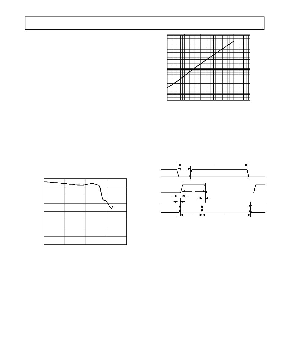
CONVERSION CONTROL
Figure 11 shows the detailed timing diagrams of the conversion
process. The AD7675 is controlled by the signal
CNVST, which
initiates conversion. Once initiated, it cannot be restarted or
aborted, even by the power-down input PD, until the conver-
sion is complete. The
CNVST signal operates independently of
CS and RD signals.
CNVST
t1
t2
MODE
ACQUIRE
CONVERT
ACQUIRE
CONVERT
t7
t8
BUSY
t4
t3
t5
t6
Figure 11. Basic Conversion Timing
For true sampling applications, the recommended operation of
the
CNVST signal is as follows:
CNVST must be held high from the previous falling edge of
BUSY, and during a minimum delay corresponding to the
acquisition time t8; then, when CNVST is brought low, a
conversion is initiated and BUSY signal goes high until the
completion of the conversion. Although
CNVST is a digital
signal, it should be designed with this special care with fast,
clean edges and levels, with minimum overshoot and under-
shoot or ringing.
For applications where the SNR is critical, the
CNVST signal should
have a very low jitter. Some solutions to achieve that are to use a
dedicated oscillator for
CNVST generation or, at least, to clock
it with a high frequency low jitter clock, as shown in Figure 5.
相关PDF资料 |
PDF描述 |
|---|---|
| P1022DS-PA | BOARD REFERENCE DESIGN P1022 |
| EVAL-AD7667CBZ | BOARD EVALUATION FOR AD7667 |
| P1020RDB-PA | BOARD REFERENCE DESIGN P1020 |
| 0210490967 | CABLE JUMPER 1.25MM .051M 27POS |
| MPC8536E-ANDROID | HARDWARE/SOFTWARE ANDROID OS |
相关代理商/技术参数 |
参数描述 |
|---|---|
| EVAL-AD7676CB | 制造商:AD 制造商全称:Analog Devices 功能描述:Evaluation Board AD766X/AD767X |
| EVAL-AD7676CBZ | 功能描述:BOARD EVALUATION FOR AD7676 RoHS:是 类别:编程器,开发系统 >> 评估板 - 模数转换器 (ADC) 系列:PulSAR® 产品培训模块:Obsolescence Mitigation Program 标准包装:1 系列:- ADC 的数量:1 位数:12 采样率(每秒):94.4k 数据接口:USB 输入范围:±VREF/2 在以下条件下的电源(标准):- 工作温度:-40°C ~ 85°C 已用 IC / 零件:MAX11645 已供物品:板,软件 |
| EVAL-AD7676EDZ | 功能描述:BOARD EVAL FOR AD7676 RoHS:是 类别:编程器,开发系统 >> 评估板 - 模数转换器 (ADC) 系列:PulSAR® 产品培训模块:Obsolescence Mitigation Program 标准包装:1 系列:- ADC 的数量:1 位数:12 采样率(每秒):94.4k 数据接口:USB 输入范围:±VREF/2 在以下条件下的电源(标准):- 工作温度:-40°C ~ 85°C 已用 IC / 零件:MAX11645 已供物品:板,软件 |
| EVAL-AD7677CB | 制造商:AD 制造商全称:Analog Devices 功能描述:Evaluation Board AD766X/AD767X |
| EVAL-AD7677CBZ | 功能描述:BOARD EVALUATION FOR AD7677 RoHS:是 类别:编程器,开发系统 >> 评估板 - 模数转换器 (ADC) 系列:PulSAR® 产品培训模块:Obsolescence Mitigation Program 标准包装:1 系列:- ADC 的数量:1 位数:12 采样率(每秒):94.4k 数据接口:USB 输入范围:±VREF/2 在以下条件下的电源(标准):- 工作温度:-40°C ~ 85°C 已用 IC / 零件:MAX11645 已供物品:板,软件 |
发布紧急采购,3分钟左右您将得到回复。