- 您现在的位置:买卖IC网 > PDF目录17038 > EVAL-AD7684CBZ (Analog Devices Inc)BOARD EVALUATION FOR AD7684 PDF资料下载
参数资料
| 型号: | EVAL-AD7684CBZ |
| 厂商: | Analog Devices Inc |
| 文件页数: | 5/16页 |
| 文件大小: | 0K |
| 描述: | BOARD EVALUATION FOR AD7684 |
| 标准包装: | 1 |
| 系列: | PulSAR® |
| ADC 的数量: | 1 |
| 位数: | 16 |
| 采样率(每秒): | 100k |
| 数据接口: | 串行 |
| 输入范围: | ±VREF |
| 在以下条件下的电源(标准): | 4mW @ 5V,100kSPS |
| 工作温度: | -40°C ~ 85°C |
| 已用 IC / 零件: | AD7684 |
| 已供物品: | 板 |
| 相关产品: | AD7684BRMZ-ND - IC ADC 16BIT 100KSPS DIFF 8MSOP AD7684BRMZRL7-ND - IC ADC 16BIT 100KSPS DIFF 8MSOP |
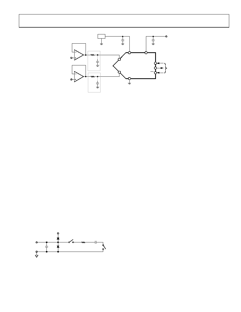
AD7684
Rev. A | Page 13 of 16
04
30
2-
02
2
AD7684
REF
GND
VDD
–IN
+IN
DCLOCK
DOUT
CS
3-WIRE INTERFACE
100nF
2.7V TO 5.25V
2.2
μF TO 10μF
(NOTE 2)
REF
0 TO VREF
33
Ω
2.7nF
(NOTE 3)
(NOTE 4)
(NOTE 1)
VREF TO 0
33
Ω
2.7nF
(NOTE 3)
(NOTE 4)
NOTE 1: SEE VOLTAGE REFERENCE INPUT SECTION FOR REFERENCE SELECTION.
NOTE 2: CREF IS USUALLY A 10μF CERAMIC CAPACITOR (X5R).
NOTE 3: SEE DRIVER AMPLIFIER CHOICE SECTION.
NOTE 4: OPTIONAL FILTER. SEE ANALOG INPUT SECTION.
NOTE 5: SEE DIGITAL INTERFACE FOR MOST CONVENIENT INTERFACE MODE.
Figure 22. Typical Application Diagram
TYPICAL CONNECTION DIAGRAM
Figure 22 shows an example of the recommended application
diagram for the AD7684.
ANALOG INPUTS
The analog inputs (+IN, IN) need to be driven differentially
180° from each other, as shown in Figure 22. Holding either
input at GND or a fixed dc gives erroneous conversion results
because the AD7684 is intended for differential operation only.
For applications requiring –IN to be at GND (±100 mV), the
AD7683 should be used.
Figure 23 shows an equivalent circuit of the input structure of
the AD7684. The two diodes, D1 and D2, provide ESD protection
for the analog inputs, +IN and IN. Care must be taken to
ensure that the analog input signal never exceeds the supply
rails by more than 0.3 V because this causes these diodes to
become forward-biased and start conducting current. However,
these diodes can handle a forward-biased current of 130 mA
maximum. For instance, these conditions could eventually
occur when the supplies of the input buffer (U1) are different
from VDD. In such a case, an input buffer with a short-circuit
current limitation can be used to protect the part.
04302-023
CIN
RIN
D1
D2
CPIN
+IN
OR –IN
GND
VDD
Figure 23. Equivalent Analog Input Circuit
This analog input structure allows the sampling of the differential
signal between +IN and IN. By using this differential input, small
signals common to both inputs are rejected. During the acquisition
phase, the impedance of the analog inputs can be modeled as a
parallel combination of the Capacitor CPIN and the network
formed by the series connection of RIN and CIN. CPIN is primarily
the pin capacitance. RIN is typically 600 Ω and is a lumped
component made up of some serial resistors and the on-
resistance of the switches. CIN is typically 30 pF and is mainly
the ADC sampling capacitor. During the conversion phase,
when the switches are opened, the input impedance is limited
to CPIN. RIN and CIN make a 1-pole, low-pass filter that reduces
undesirable aliasing effects and limits the noise.
When the source impedance of the driving circuit is low, the
AD7684 can be driven directly. Large source impedances
significantly affect the ac performance, especially THD. The dc
performances are less sensitive to the input impedance.
DRIVER AMPLIFIER CHOICE
Although the AD7684 is easy to drive, the driver amplifier
needs to meet the following requirements:
The noise generated by the driver amplifier needs to be
kept as low as possible to preserve the SNR and transition
noise performance of the AD7684. Note that the AD7684
has a noise level much lower than most other 16-bit ADCs
and, therefore, can be driven by a noisier op amp while
preserving the same or better system performance. The
noise coming from the driver is filtered by the AD7684
analog input circuit 1-pole, low-pass filter made by RIN and
CIN or by the external filter, if one is used.
For ac applications, the driver needs to have a THD
performance commensurate with the AD7684. Figure 15
shows the THD vs. frequency that the driver should exceed.
For multichannel multiplexed applications, the driver
amplifier and the AD7684 analog input circuit must be
able to settle for a full-scale step of the capacitor array at a
16-bit level (0.0015%). In the data sheet of the amplifier,
settling at 0.1% to 0.01% is more commonly specified. This
could differ significantly from the settling time at a 16-bit
level and should be verified prior to driver selection.
相关PDF资料 |
PDF描述 |
|---|---|
| HBC06DRTN-S93 | CONN EDGECARD 12POS DIP .100 SLD |
| 0210490348 | CABLE JUMPER 1.25MM .076M 28POS |
| 0210490347 | CABLE JUMPER 1.25MM .076M 28POS |
| EVAL-AD7675CBZ | BOARD EVALUATION FOR AD7675 |
| P1022DS-PA | BOARD REFERENCE DESIGN P1022 |
相关代理商/技术参数 |
参数描述 |
|---|---|
| EVAL-AD7685CB | 制造商:Analog Devices 功能描述:Evaluation Board For Use With Either The Analog Devices 制造商:Analog Devices 功能描述:EVAL FOR AD7685 - Bulk 制造商:Rochester Electronics LLC 功能描述:EVAL FOR AD7685 - Bulk |
| EVAL-AD7685CBZ | 功能描述:BOARD EVAL FOR AD7685 RoHS:是 类别:编程器,开发系统 >> 评估板 - 模数转换器 (ADC) 系列:PulSAR® 产品培训模块:Obsolescence Mitigation Program 标准包装:1 系列:- ADC 的数量:1 位数:12 采样率(每秒):94.4k 数据接口:USB 输入范围:±VREF/2 在以下条件下的电源(标准):- 工作温度:-40°C ~ 85°C 已用 IC / 零件:MAX11645 已供物品:板,软件 |
| EVAL-AD7685SDZ | 功能描述:BOARD EVAL FOR AD7685 RoHS:是 类别:编程器,开发系统 >> 评估板 - 模数转换器 (ADC) 系列:PulSAR® 产品培训模块:Obsolescence Mitigation Program 标准包装:1 系列:- ADC 的数量:1 位数:12 采样率(每秒):94.4k 数据接口:USB 输入范围:±VREF/2 在以下条件下的电源(标准):- 工作温度:-40°C ~ 85°C 已用 IC / 零件:MAX11645 已供物品:板,软件 |
| EVAL-AD7686CB | 制造商:Analog Devices 功能描述: |
| EVAL-AD7686CBZ | 功能描述:BOARD EVALUATION FOR AD7686 RoHS:是 类别:编程器,开发系统 >> 评估板 - 模数转换器 (ADC) 系列:PulSAR® 产品培训模块:Obsolescence Mitigation Program 标准包装:1 系列:- ADC 的数量:1 位数:12 采样率(每秒):94.4k 数据接口:USB 输入范围:±VREF/2 在以下条件下的电源(标准):- 工作温度:-40°C ~ 85°C 已用 IC / 零件:MAX11645 已供物品:板,软件 |
发布紧急采购,3分钟左右您将得到回复。