- 您现在的位置:买卖IC网 > PDF目录17038 > EVAL-AD7684CBZ (Analog Devices Inc)BOARD EVALUATION FOR AD7684 PDF资料下载
参数资料
| 型号: | EVAL-AD7684CBZ |
| 厂商: | Analog Devices Inc |
| 文件页数: | 6/16页 |
| 文件大小: | 0K |
| 描述: | BOARD EVALUATION FOR AD7684 |
| 标准包装: | 1 |
| 系列: | PulSAR® |
| ADC 的数量: | 1 |
| 位数: | 16 |
| 采样率(每秒): | 100k |
| 数据接口: | 串行 |
| 输入范围: | ±VREF |
| 在以下条件下的电源(标准): | 4mW @ 5V,100kSPS |
| 工作温度: | -40°C ~ 85°C |
| 已用 IC / 零件: | AD7684 |
| 已供物品: | 板 |
| 相关产品: | AD7684BRMZ-ND - IC ADC 16BIT 100KSPS DIFF 8MSOP AD7684BRMZRL7-ND - IC ADC 16BIT 100KSPS DIFF 8MSOP |
AD7684
Rev. A | Page 14 of 16
Table 9. Recommended Driver Amplifiers
Amplifier
Typical Application
Very low noise
Very low noise, single to differential
Very low noise and high frequency
Low noise and high frequency
Low power, low noise, and low frequency
5 V single-supply, low power
Small, low power, and low frequency
High frequency and low power
VOLTAGE REFERENCE INPUT
The AD7684 voltage reference input, REF, has a dynamic input
impedance. It should therefore be driven by a low impedance
source with efficient decoupling between the REF and GND
pins, as explained in more detail in the Layout section.
When REF is driven by a very low impedance source (for
example, an unbuffered reference voltage such as the low
temperature drift ADR43x reference or a reference buffer using
chip capacitor is appropriate for optimum performance.
If desired, smaller reference decoupling capacitor values down
to 2.2 μF can be used with minimal impact on performance,
especially DNL.
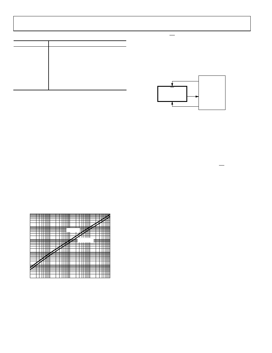
POWER SUPPLY
The AD7684 powers down automatically at the end of each
conversion phase and therefore the power scales linearly with
the sampling rate, as shown in Figure 24. This makes the part
ideal for low sampling rates (even of a few Hz) and low battery
powered applications.
0.01
0.1
1
10
100
1000
100
10
1k
10k
100k
SAMPLING RATE (SPS)
OP
E
RATING
CURRE
NT
(
μA)
04302-024
VDD = 5V
VDD = 2.7V
Figure 24. Operating Current vs. Sampling Rate
DIGITAL INTERFACE
The AD7684 is compatible with SPI, QSPI, digital hosts, and
DSPs (for example, Blackfin ADSP-BF53x or ADSP-219x). The
connection diagram is shown in Figure 25, and the corresponding
timing is given in Figure 2.
A falling edge on CS initiates a conversion and the data transfer.
After the fifth DCLOCK falling edge, DOUT is enabled and forced
low. The data bits are then clocked MSB first by subsequent
DCLOCK falling edges. The data is valid on both DCLOCK
edges. Although the rising edge can be used to capture the data,
a digital host also using the DCLOCK falling edge allows a
faster reading rate, provided it has an acceptable hold time.
04302-025
CS
DCLOCK
DOUT
DATA IN
CLK
CONVERT
DIGITAL HOST
AD7684
Figure 25. Connection Diagram
LAYOUT
The printed circuit board housing the AD7684 should be
designed so that the analog and digital sections are separated
and confined to certain areas of the board. The pinout of the
AD7684 with all its analog signals on the left side and all its
digital signals on the right side eases this task.
Avoid running digital lines under the device because these couple
noise onto the die, unless a ground plane under the AD7684 is
used as a shield. Fast switching signals, such as CS or clocks,
should never run near analog signal paths. Crossover of digital
and analog signals should be avoided.
At least one ground plane should be used. It could be common
or split between the digital and analog sections. In such a case,
it should be joined underneath the AD7684.
The AD7684 voltage reference input REF has a dynamic input
impedance and should be decoupled with minimal parasitic
inductances. This is done by placing the reference decoupling
ceramic capacitor close to, and ideally right up against, the REF
and GND pins and by connecting these pins with wide, low
impedance traces.
Finally, the power supply, VDD, of the AD7684 should be
decoupled with a ceramic capacitor, typically 100 nF, and placed
close to the AD7684. It should be connected using short and
large traces to provide low impedance paths and reduce the
effect of glitches on the power supply lines.
EVALUATING THE PERFORMANCE OF THE AD7684
Other recommended layouts for the AD7684 are outlined in the
evaluation board for the AD7684 (EVAL-AD7684CBZ). The
evaluation board package includes a fully assembled and tested
evaluation board, documentation, and software for controlling
the board from a PC via the EVAL-CONTROL BRD3Z.
相关PDF资料 |
PDF描述 |
|---|---|
| HBC06DRTN-S93 | CONN EDGECARD 12POS DIP .100 SLD |
| 0210490348 | CABLE JUMPER 1.25MM .076M 28POS |
| 0210490347 | CABLE JUMPER 1.25MM .076M 28POS |
| EVAL-AD7675CBZ | BOARD EVALUATION FOR AD7675 |
| P1022DS-PA | BOARD REFERENCE DESIGN P1022 |
相关代理商/技术参数 |
参数描述 |
|---|---|
| EVAL-AD7685CB | 制造商:Analog Devices 功能描述:Evaluation Board For Use With Either The Analog Devices 制造商:Analog Devices 功能描述:EVAL FOR AD7685 - Bulk 制造商:Rochester Electronics LLC 功能描述:EVAL FOR AD7685 - Bulk |
| EVAL-AD7685CBZ | 功能描述:BOARD EVAL FOR AD7685 RoHS:是 类别:编程器,开发系统 >> 评估板 - 模数转换器 (ADC) 系列:PulSAR® 产品培训模块:Obsolescence Mitigation Program 标准包装:1 系列:- ADC 的数量:1 位数:12 采样率(每秒):94.4k 数据接口:USB 输入范围:±VREF/2 在以下条件下的电源(标准):- 工作温度:-40°C ~ 85°C 已用 IC / 零件:MAX11645 已供物品:板,软件 |
| EVAL-AD7685SDZ | 功能描述:BOARD EVAL FOR AD7685 RoHS:是 类别:编程器,开发系统 >> 评估板 - 模数转换器 (ADC) 系列:PulSAR® 产品培训模块:Obsolescence Mitigation Program 标准包装:1 系列:- ADC 的数量:1 位数:12 采样率(每秒):94.4k 数据接口:USB 输入范围:±VREF/2 在以下条件下的电源(标准):- 工作温度:-40°C ~ 85°C 已用 IC / 零件:MAX11645 已供物品:板,软件 |
| EVAL-AD7686CB | 制造商:Analog Devices 功能描述: |
| EVAL-AD7686CBZ | 功能描述:BOARD EVALUATION FOR AD7686 RoHS:是 类别:编程器,开发系统 >> 评估板 - 模数转换器 (ADC) 系列:PulSAR® 产品培训模块:Obsolescence Mitigation Program 标准包装:1 系列:- ADC 的数量:1 位数:12 采样率(每秒):94.4k 数据接口:USB 输入范围:±VREF/2 在以下条件下的电源(标准):- 工作温度:-40°C ~ 85°C 已用 IC / 零件:MAX11645 已供物品:板,软件 |
发布紧急采购,3分钟左右您将得到回复。