- 您现在的位置:买卖IC网 > PDF目录17038 > EVAL-AD7693CBZ (Analog Devices Inc)BOARD EVALUATION FOR AD7693 PDF资料下载
参数资料
| 型号: | EVAL-AD7693CBZ |
| 厂商: | Analog Devices Inc |
| 文件页数: | 8/24页 |
| 文件大小: | 0K |
| 描述: | BOARD EVALUATION FOR AD7693 |
| 标准包装: | 1 |
| 系列: | PulSAR® |
| ADC 的数量: | 1 |
| 位数: | 16 |
| 采样率(每秒): | 500k |
| 数据接口: | 串行 |
| 输入范围: | ±VREF |
| 在以下条件下的电源(标准): | 18mW @ 500kSPS |
| 工作温度: | -40°C ~ 85°C |
| 已用 IC / 零件: | AD7693 |
| 已供物品: | 板 |
| 相关产品: | AD7693BRMZRL7-ND - IC ADC 16BIT 500KSPS 10-MSOP AD7693BCPZRL7TR-ND - IC ADC 16BIT 500KSPS 10-LFCSP AD7693BRMZ-ND - IC ADC 16BIT 500KSPS 10-MSOP AD7693BCPZRL-ND - IC ADC 16BIT 500KSPS 10LFCSP |
AD7693
Rev. A | Page 16 of 24
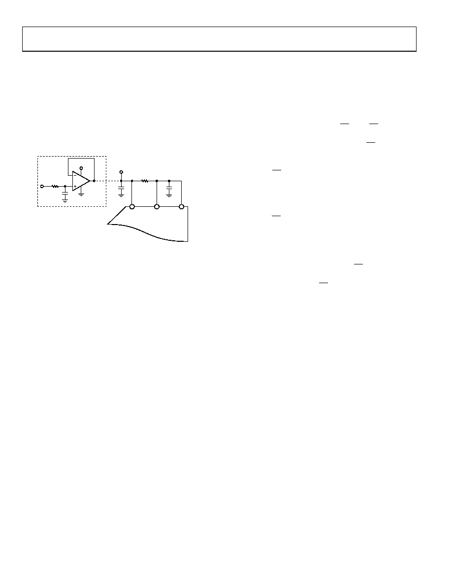
SUPPLYING THE ADC FROM THE REFERENCE
For simplified applications, the AD7693, with its low operating
current, can be supplied directly using the reference circuit
shown in Figure 33. The reference line can be driven by
The system power supply directly
A reference voltage with enough current output capability,
such as the ADR43x
A reference buffer, such as the AD8031, which can also
filter the system power supply, as shown in Figure 33
AD8031
AD7693
VIO
REF
VDD
10F
1F
10
10k
5V
1F
1
1OPTIONAL REFERENCE BUFFER AND FILTER.
06
39
4-
03
2
Figure 33. Example of an Application Circuit
DIGITAL INTERFACE
Generally, a user is interested in either minimizing the wiring
complexity of a multichannel ADC system or communicating
with the parts via a specific interface standard. Although the
ADC has only four digital pins (CNV, SCK, SDI, and SDO), it
offers a significantly flexible serial interface, including
compatibility with SPI, QSPI, digital hosts, and DSPs (such as
Blackfin ADSP-BF53x or ADSP-219x). By configuring the
ADC into one of six modes, virtually any serial interface
scenario can be accommodated.
For wiring efficiency, the best way to configure a multichannel,
simultaneous-sampling system is to use the 3-wire chain mode.
This system is easily created by cascading multiple (M) ADCs
into a shift register structure. The CNV and CLK pins are
common to all ADCs, and the SDO of one part feeds the SDI of
the next part in the chain. The 3-wire interface is simply the
CNV, SCK, and SDO of the last ADC in the chain. For a system
containing M- and N-bit converters, the user needs to provide
M × N SCK transitions to read back all of the data. This 3-wire
interface is also ideally suited for isolated applications.
Additional flexibility is provided by optionally configuring the
ADCs to provide a busy indication. Without a busy indication,
the user must externally timeout the maximum ADC
conversion time before commencing readback. This
configuration is described in the Chain Mode Without Busy
Indicator section. With the busy indication enabled, external
timer circuits are not required because the SDO at the end of
the chain provides a low-to-high transition (that is, a start bit)
when all of the chain members have completed their
conversions and are ready to transmit data. However, one
additional SCK is required to flush the SDO busy indication
prior to reading back the data. This configuration is described
in the Chain Mode with Busy Indicator section.
The primary limitations of 3-wire chain mode are that all ADCs
are simultaneously sampled and the user cannot randomly
select an individual ADC for readback. This can be overcome
only by increasing the number of wires (for example, one chip
select wire per ADC). To operate with this increased
functionality, the part must be used in CS Mode. CS mode is
separated into two categories (3-wire and 4-wire) whereby
flexibility is traded off for wiring complexity. In CS 4-wire
mode, the user has independent control over the sampling
operation (via CNV) and the chip select operation (via SDI) for
each ADC. In CS 3-wire mode, SDI is unused (tied high) and
CNV is used to both sample the input and chip select the part
when needed. As with chain mode, the parts can optionally be
configured to provide a busy indication, but at the expense of
one additional SCK when reading back the data. So in total
there are four CS modes: 3-wire and 4-wire modes, each with
busy and without busy.
There is no elaborate writing of configuration words into the
part via the SDI pin. The mode in which the part operates is
defined by ensuring a specific relationship between the CNV,
SDI, and SCK inputs at key times. To select CS mode, ensure
that SDI is high at the rising edge of CNV; otherwise, chain
mode will be selected. Once in CS mode, selecting the part for
readback before the conversion is complete (by bringing either
SDI or CNV low) instructs the part to provide a busy indicator,
a high-to-low impedance transition on SDO, to tell the user
when the conversion has finished. If the part is selected after the
conversion has finished, SDO outputs the MSB when it is
selected. In chain mode, the busy indicator, a low-to-high
transition on SDO, is selected based on the state of SCK at the
rising edge of CNV. If SCK is high, the busy indicator is
enabled; otherwise, the busy indicator is not enabled.
The following sections provide specifics for each of the different
serial interface modes. Note that in the following sections, the
timing diagrams indicate digital activity (SCK, CNV) during
conversion. However, due to the possibility of performance
degradation, digital activity should only occur during the first
quarter of the conversion phase because the AD7693 provides
error correction circuitry that can correct for an incorrect bit
during this time. The user should initiate the busy indicator if
desired during this time. It is also possible to corrupt the sample
by having SCK or SDI transitions near the sampling instant.
Therefore, it is recommended to keep the digital pins quiet for
approximately 30 ns before and 10 ns after the rising edge of
CNV. The exception is when the device is in the chain mode
with busy configuration, where SDI is tied to CNV, because this
scenario does not yield a corrupted sample. To this extent, it is
recommended, to use a discontinuous SCK whenever possible to
avoid any potential performance degradation.
相关PDF资料 |
PDF描述 |
|---|---|
| EVAL-AD7676CBZ | BOARD EVALUATION FOR AD7676 |
| LGU2W820MELZ | CAP ALUM 82UF 450V 20% SNAP |
| EBM22DCMN-S288 | CONN EDGECARD 44POS .156 EXTEND |
| MPC8306-SOM | MODULE BOARD FOR MPC830X |
| EVAL-AD7610CBZ | BOARD EVALUATION FOR AD7610 |
相关代理商/技术参数 |
参数描述 |
|---|---|
| EVAL-AD7693SDZ | 功能描述:数据转换 IC 开发工具 EVAL BOARD 16-bit ADC 500kSPS RoHS:否 制造商:Texas Instruments 产品:Demonstration Kits 类型:ADC 工具用于评估:ADS130E08 接口类型:SPI 工作电源电压:- 6 V to + 6 V |
| EVAL-AD7694CB | 制造商:Analog Devices 功能描述: |
| EVAL-AD7694CB1 | 制造商:AD 制造商全称:Analog Devices 功能描述:16-Bit, 250 kSPS PulSAR ADC in MSOP |
| EVAL-AD7694CBZ | 功能描述:BOARD EVALUATION FOR AD7694 RoHS:是 类别:编程器,开发系统 >> 评估板 - 模数转换器 (ADC) 系列:PulSAR® 产品培训模块:Obsolescence Mitigation Program 标准包装:1 系列:- ADC 的数量:1 位数:12 采样率(每秒):94.4k 数据接口:USB 输入范围:±VREF/2 在以下条件下的电源(标准):- 工作温度:-40°C ~ 85°C 已用 IC / 零件:MAX11645 已供物品:板,软件 |
| EVAL-AD7694SDZ | 功能描述:数据转换 IC 开发工具 EVALUATION BOARD RoHS:否 制造商:Texas Instruments 产品:Demonstration Kits 类型:ADC 工具用于评估:ADS130E08 接口类型:SPI 工作电源电压:- 6 V to + 6 V |
发布紧急采购,3分钟左右您将得到回复。