- 您现在的位置:买卖IC网 > PDF目录17031 > EVAL-AD7723CBZ (Analog Devices Inc)BOARD EVALUATION FOR AD7723 PDF资料下载
参数资料
| 型号: | EVAL-AD7723CBZ |
| 厂商: | Analog Devices Inc |
| 文件页数: | 10/32页 |
| 文件大小: | 0K |
| 描述: | BOARD EVALUATION FOR AD7723 |
| 标准包装: | 1 |
| ADC 的数量: | 1 |
| 位数: | 16 |
| 采样率(每秒): | 1.2M |
| 数据接口: | 串行,并联 |
| 输入范围: | ±VREF |
| 在以下条件下的电源(标准): | 475mW @ 1.2MSPS |
| 工作温度: | -40°C ~ 85°C |
| 已用 IC / 零件: | AD7723 |
| 已供物品: | 板,CD |
| 相关产品: | AD7723BSZ-REEL-ND - IC ADC 16BIT SIGMA-DELTA 44MQFP AD7723BSZ-ND - IC ADC 16BIT SIGMA-DELTA 44MQFP |
第1页第2页第3页第4页第5页第6页第7页第8页第9页当前第10页第11页第12页第13页第14页第15页第16页第17页第18页第19页第20页第21页第22页第23页第24页第25页第26页第27页第28页第29页第30页第31页第32页
AD7723
Rev. C | Page 18 of 32
CIRCUIT DESCRIPTION
The AD7723 ADC employs a Σ-Δ conversion technique to
convert the analog input into an equivalent digital word. The
modulator samples the input waveform and outputs an
equivalent digital word at the input clock frequency, fCLKIN.
Due to the high oversampling rate that spreads the quantization
noise from 0 to fCLKIN/2, the noise energy contained in the band
of interest is reduced (Figure 27A). To further reduce the
quantization noise, a high-order modulator is employed to
shape the noise spectrum so that most of the noise energy is
shifted out of the band of interest (Figure 27B).
The digital filter that follows the modulator removes the large
out-of-band quantization noise (Figure 27C) while also
reducing the data rate from fCLKIN at the input of the filter to
fCLKIN/32 or fCLKIN/16 at the output of the filter, depending on the
state on the MODE1/MODE2 pins in parallel interface mode or
the SLDR pin in serial interface mode. The AD7723 output data
rate is a little over twice the signal bandwidth, which guarantees
that there is no loss of data in the signal band.
Digital filtering has certain advantages over analog filtering.
First, since digital filtering occurs after the A/D conversion, it
can remove noise injected during the conversion process.
Analog filtering cannot remove noise injected during
conversion. Second, the digital filter combines low pass-band
ripple with a steep roll-off while also maintaining a linear phase
response.
NOISE SHAPING
QUANTIZATION NOISE
DIGITAL FILTER CUTOFF FREQUENCY
fCLKIN/2
BAND OF INTEREST
A
B
C
01186-027
fCLKIN/2
Figure 27. Sigma-Delta ADC
The AD7723 employs four or five finite impulse response (FIR)
filters in series. Each individual filter’s output data rate is half
that of the filter’s input data rate. When data is fed to the
interface from the output of the fourth filter, the output data
rate is fCLKIN/16 and the resulting oversampling ratio (OSR) of
the converter is 16. Data fed to the interface from the output of
the fifth filter results in an output data rate of fCLKIN/32 and a
corresponding OSR for the converter of 32. When an output
data rate (ODR) of fCLKIN/32 is selected, the digital filter
response can be set to either low-pass or band-pass. The band-
pass response is useful when the input signal is band limited
because the resulting output data rate is half that required to
convert the band when the low-pass operating mode is used. To
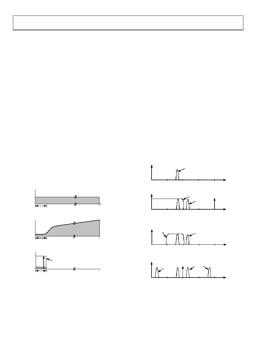
illustrate the operation of this mode, consider a band-limited
signal, as shown in Figure 28A. This signal band can be
correctly converted by selecting the (low-pass) ODR = fCLKIN/16
mode, as shown in Figure 28B. Note that the output data rate is a
little over twice the maximum frequency in the frequency band.
Alternatively, the band-pass mode can be selected, as shown in
Figure 28C. The band-pass filter removes unwanted signals
from dc to just below fCLKIN/64. Rather than outputting data at
fCLKIN/16, the output of the band-pass filter is sampled at
fCLKIN/32. This effectively translates the wanted band to a
maximum frequency of a little less than fCLKIN/64, as shown in
Figure 28D. Halving the output data rate reduces the workload
of any following signal processor and also allows a lower serial
clock rate to be used.
BAND LIMITED SIGNAL
0dB
ODR
LOW-PASS FILTER RESPONSE
SAMPLE
IMAGE
LOW-PASS FILTER. OUTPUT DATA RATE = fCLKIN/16
0dB
SAMPLE
IMAGE
BAND-PASS FILTER
RESPONSE
BAND-PASS FILTER
fCLKIN/16
LOW-PASS FILTER. OUTPUT DATA RATE =
fCLKIN/32
ODR
SAMPLE
IMAGE
FREQUENCY
TRANSLATED
INPUT SIGNAL
0dB
A
B
C
D
01186-028
fCLKIN/16
Figure 28. Band-Pass Operation
The frequency response of the three digital filter operating
modes is shown in Figure 29, Figure 30, and Figure 31.
相关PDF资料 |
PDF描述 |
|---|---|
| MLG1005S43NJ | INDUCTOR MULTILAYER 43NH 0402 |
| LLS2G101MELY | CAP ALUM 100UF 400V 20% SNAP |
| UPT2G181MRD | CAP ALUM 180UF 400V 20% RADIAL |
| STD17W-Z | WIRE & CABLE MARKERS |
| STD17W-9 | WIRE & CABLE MARKERS |
相关代理商/技术参数 |
参数描述 |
|---|---|
| EVAL-AD7725CB | 制造商:Analog Devices 功能描述:EVALUATION BOARD I.C. - Bulk 制造商:Rochester Electronics LLC 功能描述: |
| EVAL-AD7725CBZ | 功能描述:BOARD EVALUATION FOR AD7725 RoHS:是 类别:编程器,开发系统 >> 评估板 - 模数转换器 (ADC) 系列:- 产品培训模块:Obsolescence Mitigation Program 标准包装:1 系列:- ADC 的数量:1 位数:12 采样率(每秒):94.4k 数据接口:USB 输入范围:±VREF/2 在以下条件下的电源(标准):- 工作温度:-40°C ~ 85°C 已用 IC / 零件:MAX11645 已供物品:板,软件 |
| EVAL-AD7730EB | 制造商:Analog Devices 功能描述:EVALUATION BOARD I.C. - Bulk |
| EVAL-AD7730EBZ | 功能描述:BOARD EVAL FOR AD7730 RoHS:是 类别:编程器,开发系统 >> 评估板 - 模数转换器 (ADC) 系列:- 产品培训模块:Obsolescence Mitigation Program 标准包装:1 系列:- ADC 的数量:1 位数:12 采样率(每秒):94.4k 数据接口:USB 输入范围:±VREF/2 在以下条件下的电源(标准):- 工作温度:-40°C ~ 85°C 已用 IC / 零件:MAX11645 已供物品:板,软件 |
| EVAL-AD7730LEB | 制造商:Analog Devices 功能描述:EVALUATION BOARD I.C. - Bulk |
发布紧急采购,3分钟左右您将得到回复。