参数资料
| 型号: | EVAL-AD7741/42EBZ |
| 厂商: | Analog Devices Inc |
| 文件页数: | 8/12页 |
| 文件大小: | 0K |
| 描述: | BOARD EVAL FOR AD7741/7742 |
| 标准包装: | 1 |
| 主要目的: | 接口,电压至频率 |
| 嵌入式: | 否 |
| 已用 IC / 零件: | AD7741,AD7742 |
| 主要属性: | 2 个设备:第 1 个带 0~2.5 V 单端输入,第 2 个带 2 个 0~3.5 V 差分输入 |
| 次要属性: | 3072kHz 全量程内部/外部基准选项 |
| 已供物品: | 板 |
| 相关产品: | AD7741YRZ-ND - IC CONVERTER VOLT TO FREQ 8SOIC AD7741BNZ-ND - IC CONVERTER VOLT TO FREQ 8DIP AD7741BRZ-REEL7-ND - IC CONVERTER VOLT TO FREQ 8SOIC AD7741BRZ-REEL-ND - IC CONVERTER VOLT TO FREQ 8SOIC AD7741BRZ-ND - IC CONVERTER V TO FREQ 8-SOIC AD7741YR-REEL7-ND - IC CONVERTER V TO FREQ 8-SOIC AD7741YR-REEL-ND - IC CONVERTER V TO FREQ 8-SOIC AD7741BR-REEL7-ND - IC CONVERTER V TO FREQ 8-SOIC AD7741BR-REEL-ND - IC CONVERTER V TO FREQ 8-SOIC AD7741BR-ND - IC CONVERTER V TO FREQ 8-SOIC |
�� �
�
�AD7741/AD7742�
�Table� II.� AD7741/AD7742� Input� Range� Selection�
�UNI/� BIP�
�N/A�
�0�
�0�
�1�
�1�
�GAIN�
�N/A�
�0�
�1�
�0�
�1�
�Gain,� G�
�X1�
�X1�
�X2�
�X1�
�X2�
�V� IN� (Min)�
�f� OUT� =� 0.05� f� CLKIN�
�0�
�–V� REF�
�–V� REF� /2�
�0�
�0�
�V� IN� (Max)�
�f� OUT� =� 0.45� f� CLKIN�
�+V� REF�
�+V� REF�
�+V� REF� /2�
�+V� REF�
�+V� REF� /2�
�Part�
�AD7741�
�AD7742�
�AD7742�
�AD7742�
�AD7742�
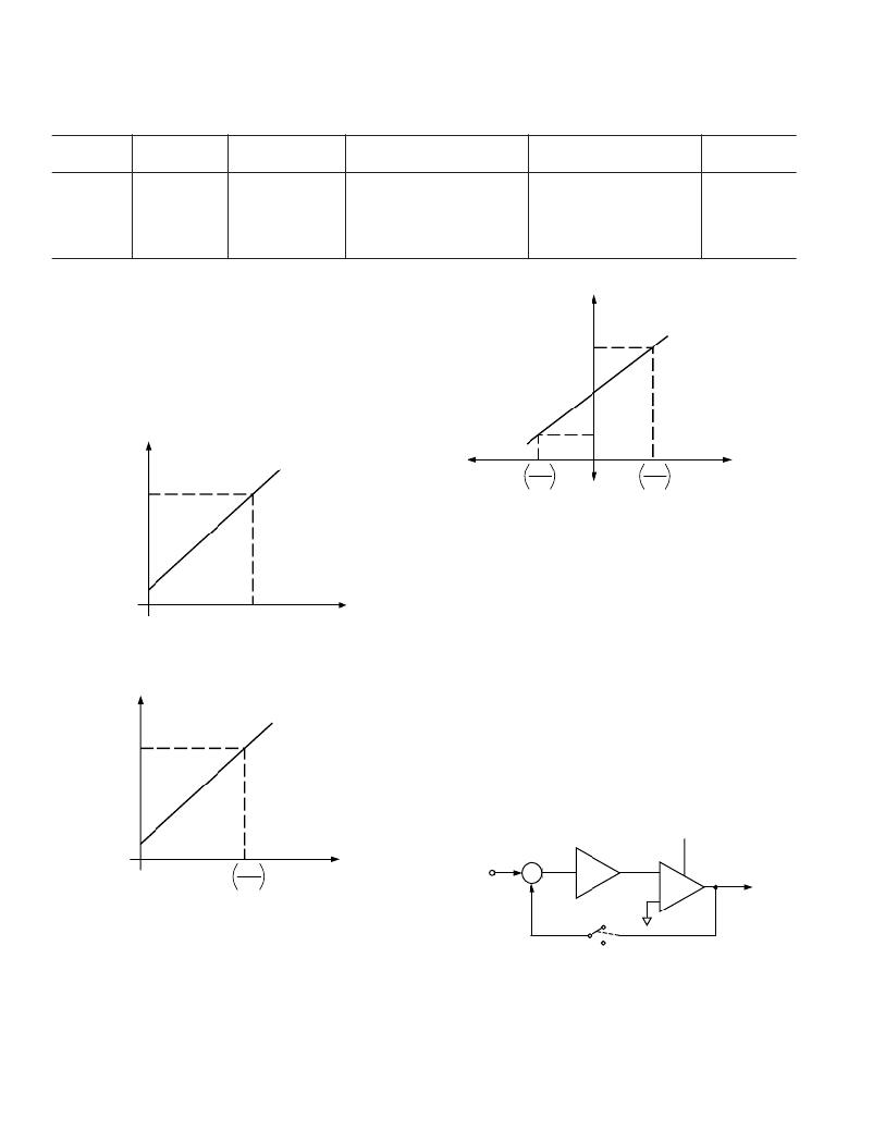
�As� can� be� seen� from� Table� II,� the� AD7741� has� one� input� range�
�configuration� whereas� the� AD7742� has� unipolar/bipolar� as�
�well� as� gain� options� depending� on� the� status� of� the� GAIN�
�and� UNI/� BIP� pins.�
�The� transfer� function� for� the� AD7741� is� shown� in� Figure� 3.�
�Figure� 4� shows� the� AD7742� transfer� function� for� unipolar� input�
�range� configuration� while� the� AD7742� transfer� function� for�
�bipolar� input� range� configuration� is� shown� in� Figure� 5.�
�OUTPUT�
�FREQUENCY�
�f� OUT�
�OUTPUT�
�FREQUENCY�
�f� OUT�
�f� OUT� MAX�
�(0.45� f� CLKIN� )�
�f� OUT� MIN�
�(0.05� f� CLKIN� )�
�f� OUT� MAX�
�–�
�V� REF�
�GAIN�
�+�
�V� REF�
�GAIN�
�DIFFERENTIAL�
�INPUT� VOLTAGE�
�(0.45� f� CLKIN� )�
�Figure� 5.� AD7742� Transfer� Characteristic� for� Bipolar�
�Differential� Input� Range:� –V� REF� /Gain� to� +V� REF� /Gain;� the�
�common-mode� range� must� be� between� +0.5� V� and�
�V� DD� –� 1.75� V.� UNI/� BIP� pin� tied� to� GND.�
�f� OUT� MIN�
�(0.05� f� CLKIN� )�
�0�
�REFIN�
�INPUT�
�VOLTAGE� V� IN�
�VFC� Modulator�
�The� analog� input� signal� to� the� AD7741/AD7742� is� continu-�
�ously� sampled� by� a� switched� capacitor� modulator� whose� sam-�
�pling� rate� is� set� by� a� master� clock� input� that� may� be� supplied�
�Figure� 3.� AD7741� Transfer� Characteristic� for� Input� Range�
�from� 0� to� V� REF�
�OUTPUT�
�FREQUENCY�
�f� OUT�
�f� OUT� MAX�
�(0.45� f� CLKIN� )�
�f� OUT� MIN�
�(0.05� f� CLKIN� )�
�externally� or� by� a� crystal-controlled� on-chip� clock� oscillator.�
�However,� the� input� signal� is� buffered� on-chip� before� being� ap-�
�plied� to� the� sampling� capacitor� of� the� modulator.� This� isolates�
�the� sampling� capacitor� charging� currents� from� the� analog� input�
�pins.�
�This� system� is� a� negative� feedback� loop� that� tries� to� keep� the� net�
�charge� on� the� integrator� capacitor� at� zero,� by� balancing� charge�
�injected� by� the� input� voltage� with� charge� injected� by� the� V� REF� .�
�The� output� of� the� comparator� provides� the� digital� input� for� the�
�1-bit� DAC,� so� that� the� system� functions� as� a� negative� feedback�
�loop� that� tries� to� minimize� the� difference� signal� (see� Figure� 6).�
�CLK�
�INTEGRATOR�
�COMPARATOR�
�0�
�+�
�V� REF�
�GAIN�
�DIFFERENTIAL�
�INPUT� VOLTAGE�
�INPUT�
�+�
�–�
�+�
�1-BIT�
�STREAM�
�Figure� 4.� AD7742� Transfer� Characteristic� for� Unipolar�
�Differential� Input� Range:� 0� V� to� V� REF� /Gain;� the� input�
�common-mode� range� must� be� between� +0.5� V� and�
�V� DD� –� 1.75� V.� UNI/� BIP� pin� tied� to� V� DD� .�
�–8� –�
�–�
�+V� REF�
�–V� REF�
�Figure� 6.� AD7741/AD7742� Modulator� Loop�
�REV.� 0�
�相关PDF资料 |
PDF描述 |
|---|---|
| EVAL-AD8003-3CPEZ | BOARD EVALUATION AD8003-3CPEZ |
| EVAL-AD9830EBZ | BOARD EVALUATION AD9830 |
| EVAL-AD9833SDZ | BOARD EVAL FOR AD9833 |
| EVAL-AD9834SDZ | BOARD EVAL FOR AD9834 |
| EVAL-ADAU1401AEBZ | BOARD EVAL FOR ADAU1401A |
相关代理商/技术参数 |
参数描述 |
|---|---|
| EVAL-AD7746EB | 制造商:AD 制造商全称:Analog Devices 功能描述:24-Bit Capacitance-to-Digital Converter with Temperature Sensor |
| EVAL-AD7746EBZ | 功能描述:BOARD EVALUATION FOR AD7746 RoHS:是 类别:编程器,开发系统 >> 评估板 - 传感器 系列:- 产品培训模块:Lead (SnPb) Finish for COTS Obsolescence Mitigation Program 标准包装:1 系列:- |
| EVAL-AD7747EBZ | 功能描述:BOARD EVAL FOR AD7747 RoHS:是 类别:编程器,开发系统 >> 评估板 - 传感器 系列:- 产品培训模块:Lead (SnPb) Finish for COTS Obsolescence Mitigation Program 标准包装:1 系列:- |
| EVAL-AD7751EB | 制造商:AD 制造商全称:Analog Devices 功能描述:Energy Metering IC With On-Chip Fault Detection |
| EVAL-AD7755EB | 制造商:AD 制造商全称:Analog Devices 功能描述:Energy Metering IC with Pulse Output |
发布紧急采购,3分钟左右您将得到回复。