- 您现在的位置:买卖IC网 > PDF目录17049 > EVAL-AD7764EDZ (Analog Devices Inc)BOARD EVAL AD7764 PDF资料下载
参数资料
| 型号: | EVAL-AD7764EDZ |
| 厂商: | Analog Devices Inc |
| 文件页数: | 20/33页 |
| 文件大小: | 0K |
| 描述: | BOARD EVAL AD7764 |
| 标准包装: | 1 |
| ADC 的数量: | 1 |
| 位数: | 24 |
| 采样率(每秒): | 312k |
| 数据接口: | 串行 |
| 输入范围: | ±3.2768 V |
| 在以下条件下的电源(标准): | 300mW @ 312kSPS |
| 工作温度: | -40°C ~ 85°C |
| 已用 IC / 零件: | AD7764 |
| 已供物品: | 板,CD |
第1页第2页第3页第4页第5页第6页第7页第8页第9页第10页第11页第12页第13页第14页第15页第16页第17页第18页第19页当前第20页第21页第22页第23页第24页第25页第26页第27页第28页第29页第30页第31页第32页第33页
AD7764
Rev. A | Page 26 of 32
CLOCKING THE AD7764
The AD7764 requires an external low jitter clock source. This
signal is applied to the MCLK pin. An internal clock signal
(ICLK) is derived from the MCLK input signal. The ICLK
controls the internal operation of the AD7764. The maximum
ICLK frequency is 20 MHz. To generate the ICLK,
ICLK = MCLK/2
For output data rates equal to those used in audio systems, a
12.288 MHz ICLK frequency can be used. As shown in Table 6,
output data rates of 96 kHz and 48 kHz are achievable with this
ICLK frequency.
MCLK JITTER REQUIREMENTS
The MCLK jitter requirements depend on a number of factors
and are given by
20
)
(
10
2
)
(
dB
SNR
f
OSR
t
IN
rms
j
×
π
×
=
where:
OSR = oversampling ratio = fICLK/ODR.
fIN = maximum input frequency.
SNR(dB) = target SNR.
Example 1
This example can be taken from Table 6, where:
ODR = 312.5 kHz.
fICLK = 20 MHz.
fIN (max) = 156.25 kHz.
SNR = 104 dB.
ps
t
rms
j
41
.
51
10
25
.
156
2
64
2
.
5
3
)
(
=
×
π
×
=
This is the maximum allowable clock jitter for a full-scale,
156.25 kHz input tone with the given ICLK and output
data rate.
Example 2
This second example can also be taken from Table 6, where:
ODR = 48 kHz.
fICLK = 12.288 MHz.
fIN (max) = 19.2 kHz.
SNR = 109 dB.
ps
470
10
2
.
19
2
256
45
.
5
3
)
(
=
×
π
×
=
rms
j
t
The input amplitude also has an effect on these jitter figures.
For example, if the input level is 3 dB below full scale, the allow-
able jitter is increased by a factor of √2, increasing the first
example to 144.65 ps rms. This happens when the maximum
slew rate is decreased by a reduction in amplitude.
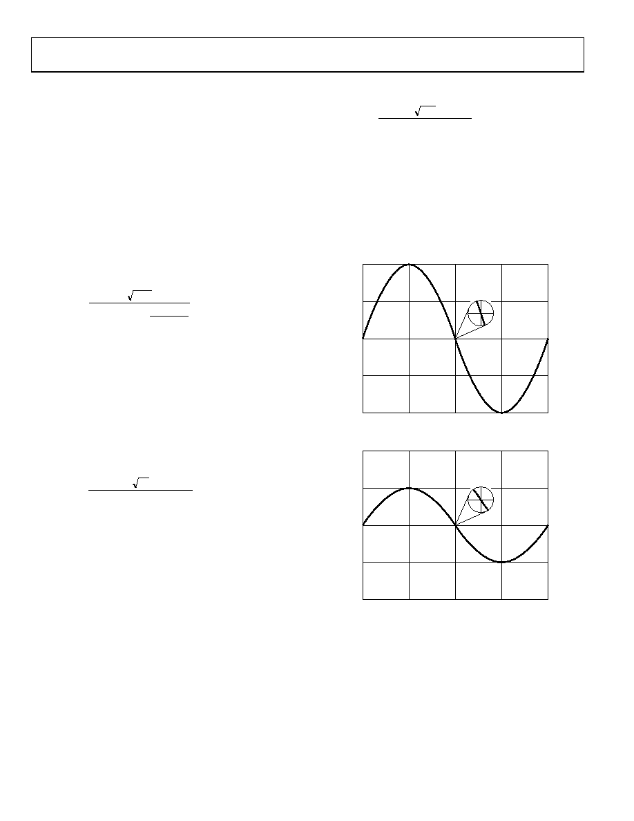
Figure 49 and Figure 50 illustrate this point, showing the
maximum slew rate of a sine wave of the same frequency but
with different amplitudes.
1.0
–1.0
0.5
0
–0.5
06518-
022
Figure 49. Maximum Slew Rate of a Sine Wave
with an Amplitude of 2 V p-p
1.0
–1.0
0.5
0
–0.5
06518-
023
Figure 50. Maximum Slew Rate of the Same Frequency Sine Wave
as in Figure 49 with an Amplitude of 1 V p-p
相关PDF资料 |
PDF描述 |
|---|---|
| STD01W-U | WIRE & CABLE MARKERS |
| DK-DEV-1AGX60N | KIT DEV ARRIA GX 1AGX60N |
| GBM25DRSS | CONN EDGECARD 50POS DIP .156 SLD |
| STD01W-C | WIRE & CABLE MARKERS |
| EVAL-AD7170EBZ | BOARD EVAL FOR AD7170 |
相关代理商/技术参数 |
参数描述 |
|---|---|
| EVAL-AD7765EBZ | 制造商:Analog Devices 功能描述:EVAL BOARD 24BIT, 312KSPS, 109DB - Bulk |
| EVAL-AD7765EDZ | 功能描述:BOARD EVAL AD7765 RoHS:是 类别:编程器,开发系统 >> 评估板 - 模数转换器 (ADC) 系列:- 产品培训模块:Obsolescence Mitigation Program 标准包装:1 系列:- ADC 的数量:1 位数:12 采样率(每秒):94.4k 数据接口:USB 输入范围:±VREF/2 在以下条件下的电源(标准):- 工作温度:-40°C ~ 85°C 已用 IC / 零件:MAX11645 已供物品:板,软件 |
| EVAL-AD7766-1EDZ | 功能描述:BOARD EVAL AD7766-1 64KSPS 111DB RoHS:是 类别:编程器,开发系统 >> 评估板 - 模数转换器 (ADC) 系列:- 产品培训模块:Obsolescence Mitigation Program 标准包装:1 系列:- ADC 的数量:1 位数:12 采样率(每秒):94.4k 数据接口:USB 输入范围:±VREF/2 在以下条件下的电源(标准):- 工作温度:-40°C ~ 85°C 已用 IC / 零件:MAX11645 已供物品:板,软件 |
| EVAL-AD7766-2EDZ | 功能描述:BOARD EVAL AD7766-2 32KSPS 114DB RoHS:是 类别:编程器,开发系统 >> 评估板 - 模数转换器 (ADC) 系列:- 产品培训模块:Obsolescence Mitigation Program 标准包装:1 系列:- ADC 的数量:1 位数:12 采样率(每秒):94.4k 数据接口:USB 输入范围:±VREF/2 在以下条件下的电源(标准):- 工作温度:-40°C ~ 85°C 已用 IC / 零件:MAX11645 已供物品:板,软件 |
| EVAL-AD7766EDZ | 功能描述:BOARD EVAL AD7766 128KSPS 108DB RoHS:是 类别:编程器,开发系统 >> 评估板 - 模数转换器 (ADC) 系列:- 产品培训模块:Obsolescence Mitigation Program 标准包装:1 系列:- ADC 的数量:1 位数:12 采样率(每秒):94.4k 数据接口:USB 输入范围:±VREF/2 在以下条件下的电源(标准):- 工作温度:-40°C ~ 85°C 已用 IC / 零件:MAX11645 已供物品:板,软件 |
发布紧急采购,3分钟左右您将得到回复。