- 您现在的位置:买卖IC网 > PDF目录17052 > EVAL-AD7922CBZ (Analog Devices Inc)BOARD EVAL FOR AD7922 PDF资料下载
参数资料
| 型号: | EVAL-AD7922CBZ |
| 厂商: | Analog Devices Inc |
| 文件页数: | 30/32页 |
| 文件大小: | 0K |
| 描述: | BOARD EVAL FOR AD7922 |
| 标准包装: | 1 |
| ADC 的数量: | 1 |
| 位数: | 12 |
| 采样率(每秒): | 1M |
| 数据接口: | 串行 |
| 输入范围: | 0 ~ Vdd |
| 在以下条件下的电源(标准): | 15.5mW @ 1MSPS,5 V |
| 工作温度: | -40°C ~ 85°C |
| 已用 IC / 零件: | AD7922 |
| 已供物品: | 板,CD |
| 相关产品: | AD7922ARMZ-REEL7-ND - IC ADC DUAL 12BIT 2CH 8MSOP AD7922AUJZ-REEL7TR-ND - IC ADC DUAL 12BIT 2CH TSOT-23-8 AD7922ARMZ-REEL-ND - IC ADC DUAL 12BIT 2CH 8MSOP AD7922ARMZ-ND - IC ADC 12BIT 1MSPS DUAL 8-MSOP |
第1页第2页第3页第4页第5页第6页第7页第8页第9页第10页第11页第12页第13页第14页第15页第16页第17页第18页第19页第20页第21页第22页第23页第24页第25页第26页第27页第28页第29页当前第30页第31页第32页
AD7912/AD7922
Rev. 0 | Page 7 of 32
TIMING SPECIFICATIONS
Guaranteed by characterization.
All input signals are specified with tr = tf = 5 ns (10% to 90% of VDD) and timed from a voltage level of 1.6 V.
VDD = 2.35 V to 5.25 V; TA = TMIN to TMAX, unless otherwise noted.
Table 3.
Parameter
Limit at TMIN,
TMAX
Unit
Description
10
kHz min2
18
MHz max
tCONVERT
16 × tSCLK
AD7922
14 × tSCLK
AD7912
tQUIET
30
ns min
Minimum quiet time required between bus relinquish and start of next conversion
t1
15
ns min
Minimum CS pulse width
t2
10
ns min
CS to SCLK setup time
t33
30
ns max
Delay from CS until DOUT three-state is disabled
t43
45
ns max
DOUT access time after SCLK falling edge
t5
0.4 tSCLK
ns min
SCLK low pulse width
t6
0.4 tSCLK
ns min
SCLK high pulse width
t74
10
ns min
SCLK to DOUT valid hold time
t8
5
ns min
DIN setup time prior to SCLK falling edge
t9
6
ns min
DIN hold time after SCLK falling edge
t105
30
ns max
SCLK falling edge to DOUT three-state
10
ns min
SCLK falling edge to DOUT three-state
tPOWER-UP6
1
s max
Power-up time from full power-down
1 Mark/space ratio for SCLK input is 40/60 to 60/40.
2 Minimum fSCLK at which specifications are guaranteed.
3 Measured with the load circuit in Figure 2 and defined as the time required for the output to cross VIH or VIL voltage.
4 Measured with a 50 pF load capacitor.
5 T10 is derived from the measured time taken by the data outputs to change 0.5 V when loaded with the circuit in Figure 2. The measured number is then extrapolated
back to remove the effects of charging or discharging the 50 pF capacitor. This means that the time, t10, quoted in the timing characteristics is the true bus relinquish
time of the part and is independent of the bus loading.
6 See the Power-Up Time section.
TIMING DIAGRAMS
04351-0-002
200
AI
OL
200
AI
OH
1.6V
TO OUTPUT
PIN
CL
50pF
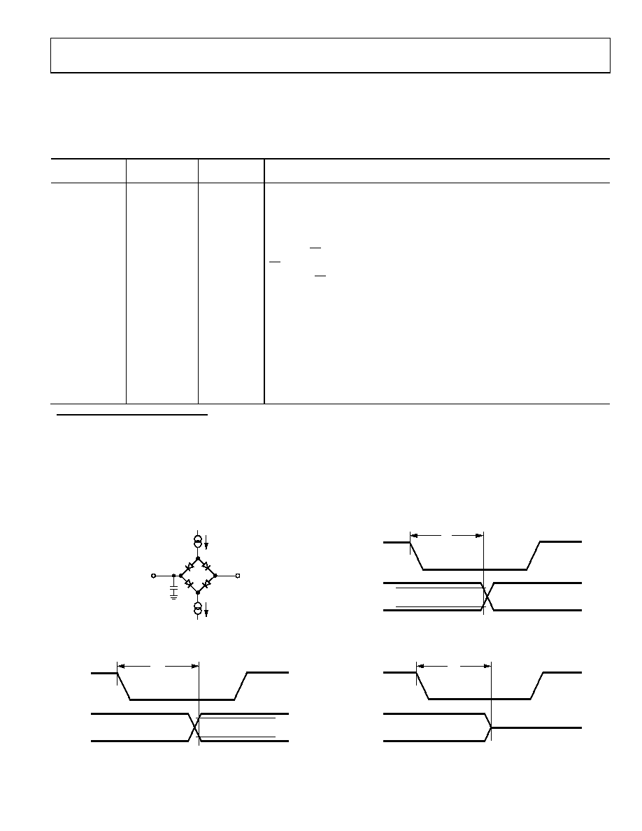
Figure 2. Load Circuit for Digital Output Timing Specifications
04351-0-003
SCLK
VIH
VIL
DOUT
t4
Figure 3. Access Time after SCLK Falling Edge
04351-0-004
SCLK
VIH
VIL
DOUT
t7
Figure 4. Hold Time after SCLK Falling Edge
04351-0-005
SCLK
1.6V
DOUT
t10
Figure 5. SCLK Falling Edge to DOUT Three-State
相关PDF资料 |
PDF描述 |
|---|---|
| EBM12DTMT-S189 | CONN EDGECARD 24POS R/A .156 SLD |
| GEM25DTMS-S189 | CONN EDGECARD 50POS R/A .156 SLD |
| VI-B3T-EY | CONVERTER MOD DC/DC 6.5V 50W |
| RCM12DTMS | CONN EDGECARD 24POS R/A .156 SLD |
| EVAL-AD7767EDZ | BOARD EVAL AD7767 128KSPS 108DB |
相关代理商/技术参数 |
参数描述 |
|---|---|
| EVAL-AD7923CB2 | 制造商:AD 制造商全称:Analog Devices 功能描述:4-Channel, 200 kSPS, 12-Bit ADC with Sequencer in 16-Lead TSSOP |
| EVAL-AD7923CBZ | 功能描述:BOARD EVAL FOR AD7923 RoHS:是 类别:编程器,开发系统 >> 评估板 - 模数转换器 (ADC) 系列:- 产品培训模块:Obsolescence Mitigation Program 标准包装:1 系列:- ADC 的数量:1 位数:12 采样率(每秒):94.4k 数据接口:USB 输入范围:±VREF/2 在以下条件下的电源(标准):- 工作温度:-40°C ~ 85°C 已用 IC / 零件:MAX11645 已供物品:板,软件 |
| EVAL-AD7927CB | 制造商:Analog Devices 功能描述:EVALUATION CONTROL BOARD. - Bulk |
| EVAL-AD7927CBZ | 功能描述:BOARD EVALUATION FOR AD7927 RoHS:是 类别:编程器,开发系统 >> 评估板 - 模数转换器 (ADC) 系列:- 产品培训模块:Obsolescence Mitigation Program 标准包装:1 系列:- ADC 的数量:1 位数:12 采样率(每秒):94.4k 数据接口:USB 输入范围:±VREF/2 在以下条件下的电源(标准):- 工作温度:-40°C ~ 85°C 已用 IC / 零件:MAX11645 已供物品:板,软件 |
| EVAL-AD7933CB | 制造商:Analog Devices 功能描述:EVALUATION BOARD 4-CHANNEL, 1.5 MSPS, 10-BIT AND 12-BIT PARALLEL ADCS WITH A SEQUENCER 制造商:Analog Devices 功能描述:EVAL BD FOR 4-CH, 1.5 MSPS, 10-BIT AND 12-BIT PARALLEL ADCS - Bulk |
发布紧急采购,3分钟左右您将得到回复。