- 您现在的位置:买卖IC网 > PDF目录17053 > EVAL-AD7940CBZ (Analog Devices Inc)BOARD EVALUATION AD7940 PDF资料下载
参数资料
| 型号: | EVAL-AD7940CBZ |
| 厂商: | Analog Devices Inc |
| 文件页数: | 10/20页 |
| 文件大小: | 0K |
| 描述: | BOARD EVALUATION AD7940 |
| 标准包装: | 1 |
| ADC 的数量: | 1 |
| 位数: | 14 |
| 采样率(每秒): | 100k |
| 数据接口: | 串行 |
| 输入范围: | 0 ~ Vdd |
| 在以下条件下的电源(标准): | 17mW @ 100kSPS & 5V |
| 工作温度: | -40°C ~ 85°C |
| 已用 IC / 零件: | AD7940 |
| 已供物品: | 板 |
| 相关产品: | AD7940BRJZ-REEL7DKR-ND - IC ADC 14BIT 100KSPS SOT-23-6 AD7940BRJZ-REEL7CT-ND - IC ADC 14BIT 100KSPS SOT-23-6 AD7940BRJZ-REEL7TR-ND - IC ADC 14BIT 100KSPS SOT-23-6 AD7940BRM-ND - IC ADC 14BIT UNIPOLAR 8-MSOP AD7940BRM-REEL7TR-ND - IC ADC 14BIT UNIPOLAR 8-MSOP |
AD7940
Rev. A | Page 18 of 20
For example, if the ADSP-2189 had a 20 MHz crystal, such that
it had a master clock frequency of 40 MHz, the master cycle
time would be 25 ns. If the SCLKDIV register is loaded with the
value 7, then a SCLK of 2.5 MHz is obtained, and 16 master
clock periods will elapse for every 1 SCLK period. Depending
on the throughput rate selected, if the timer register was loaded
with the value 803 (803 + 1 = 804), then 50.25 SCLKs will occur
between interrupts and subsequently between transmit
instructions. This situation will result in nonequidistant sampling
since the transmit instruction is occurring on a SCLK edge. If the
number of SCLKs between interrupts is a whole integer figure of N,
then equidistant sampling will be implemented by the DSP.
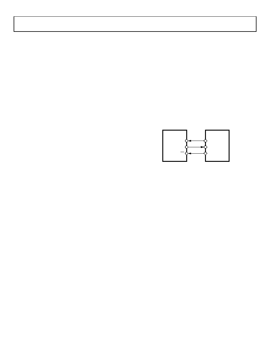
AD7940 TO DSP563xx
The connection diagram in Figure 23 shows how the AD7940
can be connected to the ESSI (synchronous serial interface) of
the DSP-563xx family of DSPs from Motorola. Each ESSI (two
on board) is operated in synchronous mode (SYN bit in CRB =
1) with internally generated 1-bit clock period frame sync for
both Tx and Rx (Bits FSL1 = 0 and FSL0 = 0 in CRB). Normal
operation of the ESSI is selected by making MOD = 0 in the
CRB. Set the word length to 16 by setting bits WL1 = 1 and
WL0 = 0 in CRA. The FSP bit in the CRB should be set to 1 so
that the frame sync is negative. It should be noted that for signal
processing applications, it is imperative that the frame
synchronization signal from the DSP-563xx provide equidistant
sampling.
In the example shown in Figure 23, the serial clock is taken from
the ESSI so the SCK0 pin must be set as an output, SCKD = 1.
03305-0-016
SCLK
AD7940*
DOUT
CS
DSP-563xx*
SCK
*ADDITIONAL PINS OMITTED FOR CLARITY
SRD
STD
Figure 23. Interfacing to the DSP-563xx
相关PDF资料 |
PDF描述 |
|---|---|
| SDR0503-822JL | INDUCTOR POWER 8200UH 5% SMD |
| VI-B20-EY | CONVERTER MOD DC/DC 5V 50W |
| VE-B1F-EY | CONVERTER MOD DC/DC 72V 50W |
| VE-B1D-EY | CONVERTER MOD DC/DC 85V 50W |
| VE-B1B-EY | CONVERTER MOD DC/DC 95V 50W |
相关代理商/技术参数 |
参数描述 |
|---|---|
| EVAL-AD7942CB | 功能描述:BOARD EVALUATION FOR AD7942 RoHS:否 类别:编程器,开发系统 >> 评估板 - 模数转换器 (ADC) 系列:PulSAR® 产品培训模块:Obsolescence Mitigation Program 标准包装:1 系列:- ADC 的数量:1 位数:12 采样率(每秒):94.4k 数据接口:USB 输入范围:±VREF/2 在以下条件下的电源(标准):- 工作温度:-40°C ~ 85°C 已用 IC / 零件:MAX11645 已供物品:板,软件 |
| EVAL-AD7942SDZ | 功能描述:BOARD EVAL FOR AD7942 RoHS:是 类别:编程器,开发系统 >> 评估板 - 模数转换器 (ADC) 系列:PulSAR® 产品培训模块:Obsolescence Mitigation Program 标准包装:1 系列:- ADC 的数量:1 位数:12 采样率(每秒):94.4k 数据接口:USB 输入范围:±VREF/2 在以下条件下的电源(标准):- 工作温度:-40°C ~ 85°C 已用 IC / 零件:MAX11645 已供物品:板,软件 |
| EVAL-AD7944EBZ | 功能描述:BOARD EVAL FOR AD7944 RoHS:是 类别:编程器,开发系统 >> 评估板 - 模数转换器 (ADC) 系列:PulSAR® 产品培训模块:Obsolescence Mitigation Program 标准包装:1 系列:- ADC 的数量:1 位数:12 采样率(每秒):94.4k 数据接口:USB 输入范围:±VREF/2 在以下条件下的电源(标准):- 工作温度:-40°C ~ 85°C 已用 IC / 零件:MAX11645 已供物品:板,软件 |
| EVAL-AD7946CBZ | 功能描述:BOARD EVALUATION FOR AD7946 RoHS:是 类别:编程器,开发系统 >> 评估板 - 模数转换器 (ADC) 系列:PulSAR® 产品培训模块:Obsolescence Mitigation Program 标准包装:1 系列:- ADC 的数量:1 位数:12 采样率(每秒):94.4k 数据接口:USB 输入范围:±VREF/2 在以下条件下的电源(标准):- 工作温度:-40°C ~ 85°C 已用 IC / 零件:MAX11645 已供物品:板,软件 |
| EVAL-AD7946SDZ | 功能描述:BOARD EVAL FOR AD7946 RoHS:否 类别:编程器,开发系统 >> 评估板 - 模数转换器 (ADC) 系列:* 产品培训模块:Obsolescence Mitigation Program 标准包装:1 系列:- ADC 的数量:1 位数:12 采样率(每秒):94.4k 数据接口:USB 输入范围:±VREF/2 在以下条件下的电源(标准):- 工作温度:-40°C ~ 85°C 已用 IC / 零件:MAX11645 已供物品:板,软件 |
发布紧急采购,3分钟左右您将得到回复。