- 您现在的位置:买卖IC网 > PDF目录17053 > EVAL-AD7940CBZ (Analog Devices Inc)BOARD EVALUATION AD7940 PDF资料下载
参数资料
| 型号: | EVAL-AD7940CBZ |
| 厂商: | Analog Devices Inc |
| 文件页数: | 9/20页 |
| 文件大小: | 0K |
| 描述: | BOARD EVALUATION AD7940 |
| 标准包装: | 1 |
| ADC 的数量: | 1 |
| 位数: | 14 |
| 采样率(每秒): | 100k |
| 数据接口: | 串行 |
| 输入范围: | 0 ~ Vdd |
| 在以下条件下的电源(标准): | 17mW @ 100kSPS & 5V |
| 工作温度: | -40°C ~ 85°C |
| 已用 IC / 零件: | AD7940 |
| 已供物品: | 板 |
| 相关产品: | AD7940BRJZ-REEL7DKR-ND - IC ADC 14BIT 100KSPS SOT-23-6 AD7940BRJZ-REEL7CT-ND - IC ADC 14BIT 100KSPS SOT-23-6 AD7940BRJZ-REEL7TR-ND - IC ADC 14BIT 100KSPS SOT-23-6 AD7940BRM-ND - IC ADC 14BIT UNIPOLAR 8-MSOP AD7940BRM-REEL7TR-ND - IC ADC 14BIT UNIPOLAR 8-MSOP |
AD7940
Rev. A | Page 17 of 20
MICROPROCESSOR INTERFACING
The serial interface on the AD7940 allows the part to be directly
connected to a range of many different microprocessors. This
section explains how to interface the AD7940 with some of the
more common microcontroller and DSP serial interface
protocols.
AD7940 TO TMS320C541
The serial interface on the TMS320C541 uses a continuous
serial clock and frame synchronization signals to synchronize
the data transfer operations with peripheral devices such as the
AD7940. The CS input allows easy interfacing between the
TMS320C541 and the AD7940 with no glue logic required. The
serial port of the TMS320C541 is set up to operate in burst
mode with internal CLKX (TX serial clock) and FSX (TX frame
sync). The serial port control register (SPC) must have the
following setup:
FO = 0
FSM = 1
MCM = 1
TXM = 1
The format bit, FO, must be set to 1 to set the word length to
8 bits, in order to implement the power-down mode on the
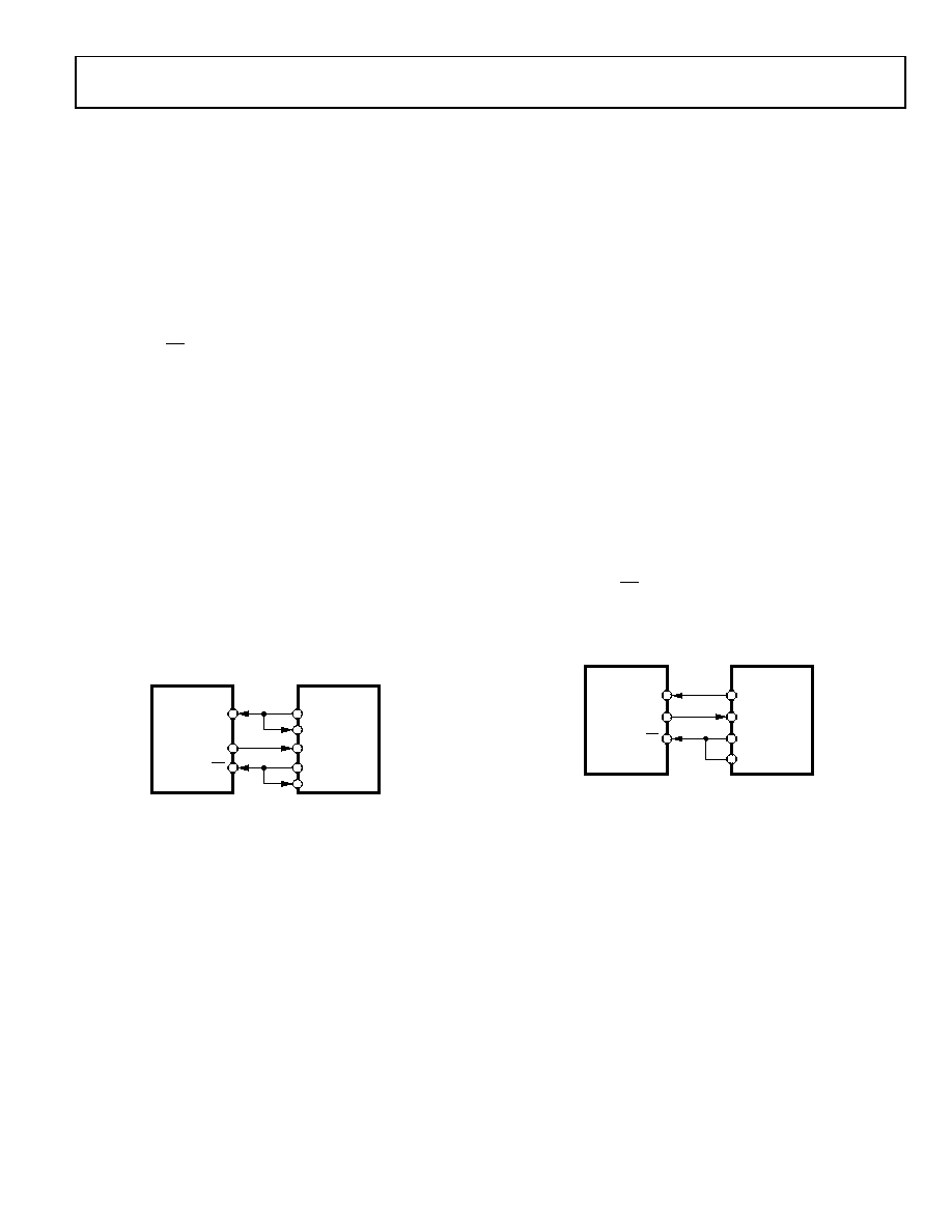
AD7940. The connection diagram is shown in Figure 21. It
should be noted that for signal processing applications, it is
imperative that the frame synchronization signal from the
TMS320C541 provide equidistant sampling.
03305-0-014
AD7940*
TMS320C541*
*ADDITIONAL PINS OMITTED FOR CLARITY
SDATA
DR
CS
FSX
FSR
SCLK
CLKX
CLKR
Figure 21. Interfacing to the TMS320C541
AD7940 TO ADSP-218x
The ADSP-218x family of DSPs can be interfaced directly to the
AD7940 with no glue logic required. The SPORT control regis-
ter should be set up as follows:
TFSW = RFSW = 1, Alternate Framing
INVRFS = INVTFS = 1, Active Low Frame Signal
DTYPE = 00, Right Justify Data
SLEN = 1111, 16-Bit Data-Words
ISCLK = 1, Internal Serial Clock
TFSR = RFSR = 0, Frame First Word
IRFS = 0
ITFS = 1
To implement power-down mode, SLEN should be set to 0111
to issue an 8-bit SCLK burst.
The connection diagram is shown in Figure 22. The ADSP-218x
has the TFS and RFS of the SPORT tied together, with TFS set
as an output and RFS set as an input. The DSP operates in
alternate framing mode, and the SPORT control register is set
up as described. The frame synchronization signal generated on
the TFS is tied to CS, and, as with all signal processing
applications, equidistant sampling is necessary. In this example,
the timer interrupt is used to control the sampling rate of the
ADC.
03305-0-015
SCLK
AD7940*
SDATA
CS
ADSP-218x*
SCLK
*ADDITIONAL PINS OMITTED FOR CLARITY
DR
RFS
TFS
Figure 22. Interfacing to the ADSP-218x
The timer register is loaded with a value that provides an
interrupt at the required sample interval. When an interrupt is
received, the values in the transmit autobuffer start to be
transmitted and TFS is generated. The TFS is used to control
the
RFS and, therefore, the reading of data. The data is stored in the
receive autobuffer for processing or to be shifted later. The
frequency of the serial clock is set in the SCLKDIV register.
When the instruction to transmit with TFS is given, i.e., TX0 =
AX0, the state of the SCLK is checked. The DSP waits until the
SCLK has gone high, low, and high before transmission will
start. If the timer and SCLK values are chosen such that the
instruction to transmit occurs on or near the rising edge of
SCLK, the data may be transmitted, or it may wait until the next
clock edge.
相关PDF资料 |
PDF描述 |
|---|---|
| SDR0503-822JL | INDUCTOR POWER 8200UH 5% SMD |
| VI-B20-EY | CONVERTER MOD DC/DC 5V 50W |
| VE-B1F-EY | CONVERTER MOD DC/DC 72V 50W |
| VE-B1D-EY | CONVERTER MOD DC/DC 85V 50W |
| VE-B1B-EY | CONVERTER MOD DC/DC 95V 50W |
相关代理商/技术参数 |
参数描述 |
|---|---|
| EVAL-AD7942CB | 功能描述:BOARD EVALUATION FOR AD7942 RoHS:否 类别:编程器,开发系统 >> 评估板 - 模数转换器 (ADC) 系列:PulSAR® 产品培训模块:Obsolescence Mitigation Program 标准包装:1 系列:- ADC 的数量:1 位数:12 采样率(每秒):94.4k 数据接口:USB 输入范围:±VREF/2 在以下条件下的电源(标准):- 工作温度:-40°C ~ 85°C 已用 IC / 零件:MAX11645 已供物品:板,软件 |
| EVAL-AD7942SDZ | 功能描述:BOARD EVAL FOR AD7942 RoHS:是 类别:编程器,开发系统 >> 评估板 - 模数转换器 (ADC) 系列:PulSAR® 产品培训模块:Obsolescence Mitigation Program 标准包装:1 系列:- ADC 的数量:1 位数:12 采样率(每秒):94.4k 数据接口:USB 输入范围:±VREF/2 在以下条件下的电源(标准):- 工作温度:-40°C ~ 85°C 已用 IC / 零件:MAX11645 已供物品:板,软件 |
| EVAL-AD7944EBZ | 功能描述:BOARD EVAL FOR AD7944 RoHS:是 类别:编程器,开发系统 >> 评估板 - 模数转换器 (ADC) 系列:PulSAR® 产品培训模块:Obsolescence Mitigation Program 标准包装:1 系列:- ADC 的数量:1 位数:12 采样率(每秒):94.4k 数据接口:USB 输入范围:±VREF/2 在以下条件下的电源(标准):- 工作温度:-40°C ~ 85°C 已用 IC / 零件:MAX11645 已供物品:板,软件 |
| EVAL-AD7946CBZ | 功能描述:BOARD EVALUATION FOR AD7946 RoHS:是 类别:编程器,开发系统 >> 评估板 - 模数转换器 (ADC) 系列:PulSAR® 产品培训模块:Obsolescence Mitigation Program 标准包装:1 系列:- ADC 的数量:1 位数:12 采样率(每秒):94.4k 数据接口:USB 输入范围:±VREF/2 在以下条件下的电源(标准):- 工作温度:-40°C ~ 85°C 已用 IC / 零件:MAX11645 已供物品:板,软件 |
| EVAL-AD7946SDZ | 功能描述:BOARD EVAL FOR AD7946 RoHS:否 类别:编程器,开发系统 >> 评估板 - 模数转换器 (ADC) 系列:* 产品培训模块:Obsolescence Mitigation Program 标准包装:1 系列:- ADC 的数量:1 位数:12 采样率(每秒):94.4k 数据接口:USB 输入范围:±VREF/2 在以下条件下的电源(标准):- 工作温度:-40°C ~ 85°C 已用 IC / 零件:MAX11645 已供物品:板,软件 |
发布紧急采购,3分钟左右您将得到回复。