- 您现在的位置:买卖IC网 > PDF目录16419 > EVAL-AD9393-AKZ (Analog Devices Inc)EVAL KIT 9393 PDF资料下载
参数资料
| 型号: | EVAL-AD9393-AKZ |
| 厂商: | Analog Devices Inc |
| 文件页数: | 15/40页 |
| 文件大小: | 0K |
| 描述: | EVAL KIT 9393 |
| 标准包装: | 1 |
| 主要目的: | 视频,开关,HDMI |
| 嵌入式: | 否 |
| 已用 IC / 零件: | AD9393 |
| 已供物品: | 板 |
第1页第2页第3页第4页第5页第6页第7页第8页第9页第10页第11页第12页第13页第14页当前第15页第16页第17页第18页第19页第20页第21页第22页第23页第24页第25页第26页第27页第28页第29页第30页第31页第32页第33页第34页第35页第36页第37页第38页第39页第40页
AD9393
Rev. 0 | Page 22 of 40
2-WIRE SERIAL CONTROL REGISTER DETAILS
This section describes certain register details. Note that not all
registers are discussed in this section.
CHIP IDENTIFICATION
0x00—Bits[7:0], Chip Revision
An 8-bit value that reflects the current chip revision.
0x17—Bits[3:0], HSYNCs per VSYNC MSB
These bits are four MSBs of the 12-bit counter that reports the
number of HSYNCs per VSYNC on the active input. This is
useful in determining the mode and aid in setting the PLL
divide ratio.
0x18—Bit[7:0], HSYNCs per VSYNC LSB
These bits are eight LSBs of the 12-bit counter that reports the
number of HSYNCs per VSYNCs on the active input.
0x23—Bits[7:0], HSYNC Duration
These bits are an 8-bit register that sets the duration of the
HSYNC output pulse. The leading edge of the HSYNC output
is triggered by the internally generated, phase-adjusted PLL
feedback clock. The AD9393 then counts a number of pixel
clocks equal to the value in this register. This triggers the
trailing edge of the HSYNC output, which is also phase-
adjusted. The power-up default is 32.
0x24—Bit[7], HSYNC Output Polarity
This bit sets the polarity of the HSYNC output. Setting this bit
to 0 sets the HSYNC output to active low. Setting this bit to 1
sets the HSYNC output to active high. The power-up default
setting is 1.
0x24—Bit[6], VSYNC Output Polarity
This bit sets the polarity of the VSYNC output. Setting this bit to 0
sets the VSYNC output to active low. Setting this bit to 1 sets the
VSYNC output to active high. The power-up default is 1.
0x24—Bit[5] DE Output Polarity
This bit sets the polarity of the display enable (DE). 0 = DE
output polarity is negative. 1 = DE output polarity is positive.
The power-up default is 1.
0x24—Bit[4], Field Output Polarity
This bit sets the polarity of the odd/even field output signal on
Ball A7. 0 = active low = even field; active high = odd field. 1 =
active high = odd field; active high = even field. The power-up
default setting is 1.
0x24—Bit[0], Output CLK Invert
This bit allows inversion of the output clock as specified by
Register 0x25, Bits[7:6]. 0 = noninverted clock. 1 = inverted
clock. The power-up default setting is 0.
0x25—Bits[7:6], Output CLK Select
These bits select the clock output on the DCLK ball. They
include × clock, a 2× clock, a 90° phase shifted clock, or
the normal pixel clock. The power-up default setting is 01.
See Table 10.
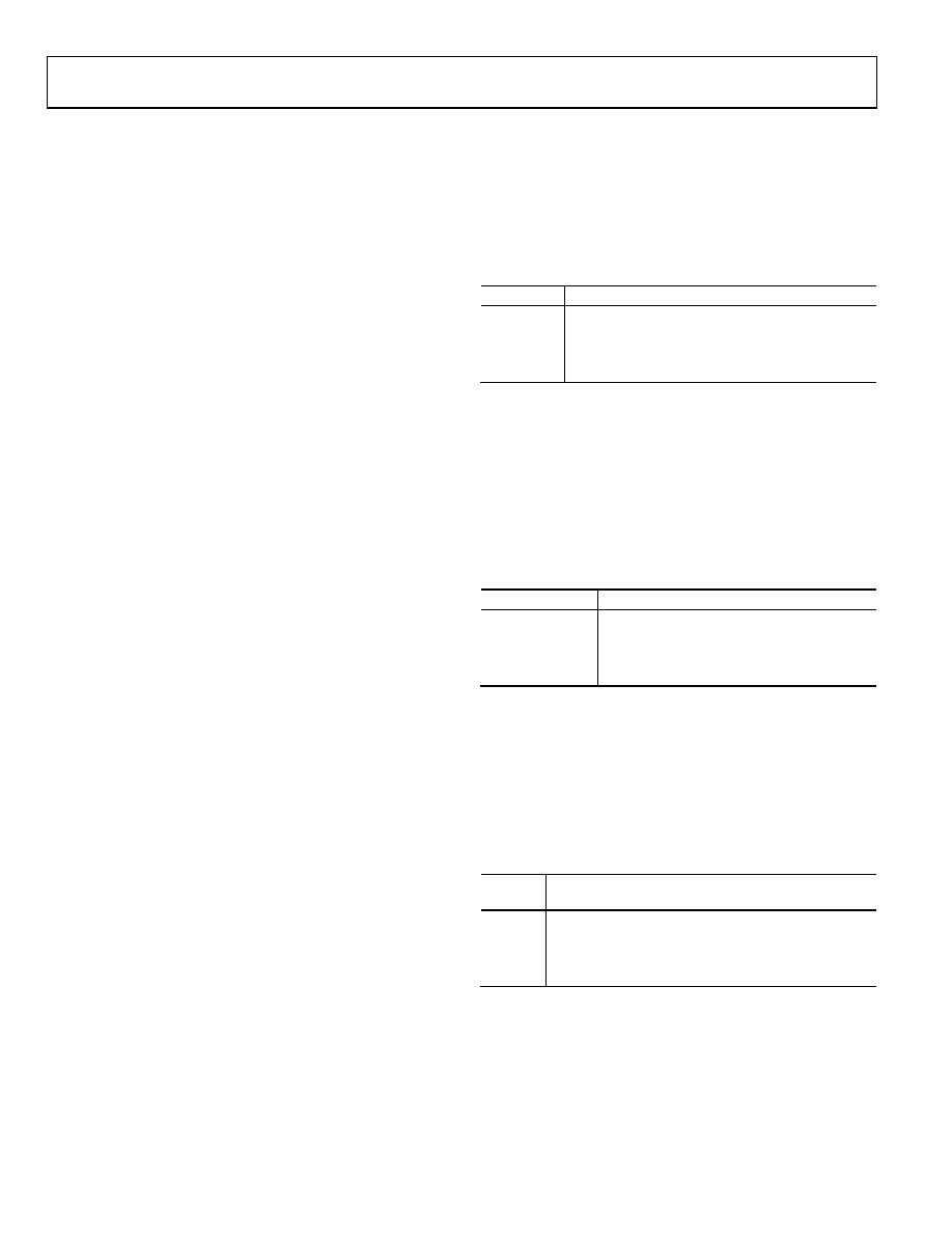
Table 10. Output Clock Select
Select
Result
00
× pixel clock
01
1× pixel clock
10
2× pixel clock
11
90° phase 1× pixel clock
0x25—Bits[5:4], Output Drive Strength
These two bits select the drive strength for all the high speed
digital outputs (except the VSOUT, HSOUT, and O/E). Higher
drive strength results in faster rise/fall times and in general
makes it easier to capture data. Lower drive strength results in
slower rise/fall times and helps to reduce EMI and digitally
generated power supply noise. The power-up default setting is
11. See Table 11.
Table 11. Output Drive Strength
Output Drive
Result
00
Low output drive strength
01
Medium low output drive strength
10
Medium high output drive strength
11
High output drive strength
0x25—Bits[3:2], Output Mode
These bits choose between four options for the output mode.
4:4:4 mode is standard RGB; 4:2:2 mode is YCrCb, which
reduces the number of active output pins from 24 to 16; 4:4:4
is double data rate (DDR) output mode; and the data is RGB
mode that changes on every clock edge. The power-up default
setting is 00. See Table 12.
Table 12. Output Mode
Output
Mode
Result
00
4:4:4 RGB mode
01
4:2:2 YCrCb mode + DDR 4:2:2 on D[7:0] (secondary)
10
DDR 4:4:4 DDR mode + DDR 4:2:2 on D[7:0] (secondary)
11
12-bit 4:2:2
相关PDF资料 |
PDF描述 |
|---|---|
| VI-JTT-EX | CONVERTER MOD DC/DC 6.5V 75W |
| VE-2WN-EX | CONVERTER MOD DC/DC 18.5V 75W |
| APX811-29UG-7 | IC SUPERVISOR 2.93V SOT143-4 |
| 2-6278127-0 | SC SIMPLX/MT-RJ 20M1 C/A |
| VE-2WM-EX | CONVERTER MOD DC/DC 10V 75W |
相关代理商/技术参数 |
参数描述 |
|---|---|
| EVAL-AD974CB | 功能描述:BOARD EVAL FOR AD974 RoHS:否 类别:编程器,开发系统 >> 评估板 - 模数转换器 (ADC) 系列:- 产品培训模块:Obsolescence Mitigation Program 标准包装:1 系列:- ADC 的数量:1 位数:12 采样率(每秒):94.4k 数据接口:USB 输入范围:±VREF/2 在以下条件下的电源(标准):- 工作温度:-40°C ~ 85°C 已用 IC / 零件:MAX11645 已供物品:板,软件 |
| EVAL-AD976ACB | 功能描述:BOARD EVAL FOR AD976A RoHS:否 类别:编程器,开发系统 >> 评估板 - 模数转换器 (ADC) 系列:- 产品培训模块:Obsolescence Mitigation Program 标准包装:1 系列:- ADC 的数量:1 位数:12 采样率(每秒):94.4k 数据接口:USB 输入范围:±VREF/2 在以下条件下的电源(标准):- 工作温度:-40°C ~ 85°C 已用 IC / 零件:MAX11645 已供物品:板,软件 |
| EVAL-AD976CB | 功能描述:BOARD EVAL FOR AD976 RoHS:否 类别:编程器,开发系统 >> 评估板 - 模数转换器 (ADC) 系列:- 产品培训模块:Obsolescence Mitigation Program 标准包装:1 系列:- ADC 的数量:1 位数:12 采样率(每秒):94.4k 数据接口:USB 输入范围:±VREF/2 在以下条件下的电源(标准):- 工作温度:-40°C ~ 85°C 已用 IC / 零件:MAX11645 已供物品:板,软件 |
| EVAL-AD977ACB | 功能描述:BOARD EVAL FOR AD977A RoHS:否 类别:编程器,开发系统 >> 评估板 - 模数转换器 (ADC) 系列:- 产品培训模块:Obsolescence Mitigation Program 标准包装:1 系列:- ADC 的数量:1 位数:12 采样率(每秒):94.4k 数据接口:USB 输入范围:±VREF/2 在以下条件下的电源(标准):- 工作温度:-40°C ~ 85°C 已用 IC / 零件:MAX11645 已供物品:板,软件 |
| EVAL-AD977CB | 功能描述:BOARD EVAL FOR AD977 RoHS:否 类别:编程器,开发系统 >> 评估板 - 模数转换器 (ADC) 系列:- 产品培训模块:Obsolescence Mitigation Program 标准包装:1 系列:- ADC 的数量:1 位数:12 采样率(每秒):94.4k 数据接口:USB 输入范围:±VREF/2 在以下条件下的电源(标准):- 工作温度:-40°C ~ 85°C 已用 IC / 零件:MAX11645 已供物品:板,软件 |
发布紧急采购,3分钟左右您将得到回复。