- 您现在的位置:买卖IC网 > PDF目录16589 > EVAL-ADCMP566BCPZ (Analog Devices Inc)BOARD EVALUATION ADCMP566BPZ PDF资料下载
参数资料
| 型号: | EVAL-ADCMP566BCPZ |
| 厂商: | Analog Devices Inc |
| 文件页数: | 13/16页 |
| 文件大小: | 0K |
| 描述: | BOARD EVALUATION ADCMP566BPZ |
| 标准包装: | 1 |
| 主要目的: | 接口,比较器 |
| 已用 IC / 零件: | ADCMP566BPZ |
| 已供物品: | 板 |
| 相关产品: | ADCMP566BCPZ-ND - IC COMP DUAL ULTRA-FAST 32LFCSP |
ADCMP566
Rev. 0 | Page 6 of 16
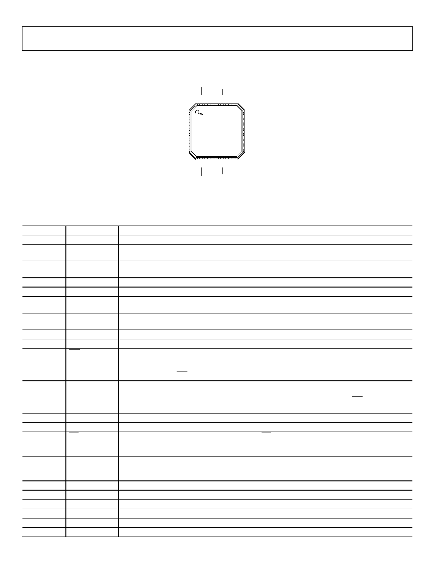
PIN CONFIGURATION AND FUNCTION DESCRIPTIONS
PIN 1
INDICATOR
VEE
24
23 NC
22 VEE
21 VCC
GND
–INA
+INA
32
GN
D
20 VCC
19 VEE
18 NC
17 VEE
GND
9
LEB
1
0
LEB
1
NC
1
2
GND
1
3
QB
14
QB
15
GND
1
6
VCC
+INB
–INB
GND
1
2
3
4
5
6
7
8
31
LEA
30
LEA
NC
29
27
QA
26
QA
25
GN
D
28
GN
D
NC = NO CONNECT
03633-0-002
ADCMP566
TOP VIEW
(Not to Scale)
Figure 2. ADCMP566 Pin Configuration
Table 3. ADCMP566 Pin Descriptions
Pin No.
Mnemonic
Function
1
GND
Analog Ground
2
INA
Inverting analog input of the differential input stage for Channel A. The inverting A input must be driven
in conjunction with the noninverting A input.
3
+INA
Noninverting analog input of the differential input stage for Channel A. The noninverting A input must
be driven in conjunction with the inverting A input.
4
VCC
Positive Supply Terminal
5
VCC
Positive Supply Terminal
6
+INB
Noninverting analog input of the differential input stage for Channel B. The noninverting B input must
be driven in conjunction with the inverting B input.
7
INB
Inverting analog input of the differential input stage for Channel B. The inverting B input must be driven
in conjunction with the noninverting B input.
8
GND
Analog Ground
9
GND
Analog Ground
10
LEB
One of two complementary inputs for Channel B Latch Enable. In the compare mode (logic low), the
output will track changes at the input of the comparator. In the latch mode (logic high), the output will
reflect the input state just prior to the comparator’s being placed in the latch mode. LEB must be driven
in conjunction with LEB.
11
LEB
One of two complementary inputs for Channel B Latch Enable. In the compare mode (logic high), the
output will track changes at the input of the comparator. In the latch mode (logic low), the output will
reflect the input state just prior to the comparator’s being placed in the latch mode. LEB must be driven
in conjunction with LEB.
12
NC
No Connect. Leave pin unconnected.
13
GND
Digital Ground
14
QB
One of two complementary outputs for Channel B. QB will be at logic low if the analog voltage at the
noninverting input is greater than the analog voltage at the inverting input (provided the comparator is
in the compare mode). See the LEB description (Pin 11) for more information.
15
QB
One of two complementary outputs for Channel B. QB will be at logic high if the analog voltage at the
noninverting input is greater than the analog voltage at the inverting input (provided the comparator is
in the compare mode). See the LEB description (Pin 11) for more information.
16
GND
Digital Ground
17
VEE
Negative Supply Terminal
18
NC
No Connect. Leave pin unconnected.
19
VEE
Negative Supply Terminal
20
VCC
Positive Supply Terminal
21
VCC
Positive Supply Terminal
相关PDF资料 |
PDF描述 |
|---|---|
| HCM11DRAI | CONN EDGECARD 22POS R/A .156 SLD |
| EVAL-ADCMP565BPZ | BOARD EVALUATION ADCMP565BPZ |
| GEM31DTKT | CONN EDGECARD 62POS DIP .156 SLD |
| GCM24DTKS | CONN EDGECARD 48POS DIP .156 SLD |
| GEM36DSXI | CONN EDGECARD 72POS DIP .156 SLD |
相关代理商/技术参数 |
参数描述 |
|---|---|
| EVAL-ADCMP567BCPZ | 功能描述:BOARD EVALUATION ADCMP567BCP RoHS:是 类别:编程器,开发系统 >> 评估演示板和套件 系列:- 标准包装:1 系列:- 主要目的:电信,线路接口单元(LIU) 嵌入式:- 已用 IC / 零件:IDT82V2081 主要属性:T1/J1/E1 LIU 次要属性:- 已供物品:板,电源,线缆,CD 其它名称:82EBV2081 |
| EVAL-ADCMP572BCP | 制造商:Analog Devices 功能描述:EVAL BOARD-SINGLE SUPPLY, CML ON XFCB3.0 - Bulk |
| EVAL-ADCMP572BCPZ | 功能描述:BOARD EVALUATION ADCMP572BCP RoHS:是 类别:编程器,开发系统 >> 评估演示板和套件 系列:- 标准包装:1 系列:- 主要目的:电信,线路接口单元(LIU) 嵌入式:- 已用 IC / 零件:IDT82V2081 主要属性:T1/J1/E1 LIU 次要属性:- 已供物品:板,电源,线缆,CD 其它名称:82EBV2081 |
| EVAL-ADCMP573BCP | 制造商:Analog Devices 功能描述:EVAL BOARDSINGLE SUPPLY, PECL ON XFCB3.0 - Bulk |
| EVAL-ADCMP573BCPZ | 功能描述:BOARD EVALUATION ADCMP573BCP RoHS:是 类别:编程器,开发系统 >> 评估演示板和套件 系列:- 标准包装:1 系列:- 主要目的:电信,线路接口单元(LIU) 嵌入式:- 已用 IC / 零件:IDT82V2081 主要属性:T1/J1/E1 LIU 次要属性:- 已供物品:板,电源,线缆,CD 其它名称:82EBV2081 |
发布紧急采购,3分钟左右您将得到回复。