- 您现在的位置:买卖IC网 > PDF目录16578 > EVAL-ADM3252EEBZ (Analog Devices Inc)BOARD EVAL FOR ADM3252E PDF资料下载
参数资料
| 型号: | EVAL-ADM3252EEBZ |
| 厂商: | Analog Devices Inc |
| 文件页数: | 2/16页 |
| 文件大小: | 0K |
| 描述: | BOARD EVAL FOR ADM3252E |
| 标准包装: | 1 |
| 主要目的: | 接口,隔离式,RS-232 |
| 嵌入式: | 否 |
| 已用 IC / 零件: | ADM3252E |
| 主要属性: | 2.5 kV 隔离式(电源和数据)RS-232 收发器,隔离式 DC/DC 转换器 |
| 次要属性: | 2 通道 |
| 已供物品: | 板 |
ADM3252E
Data Sheet
Rev. A | Page 10 of 16
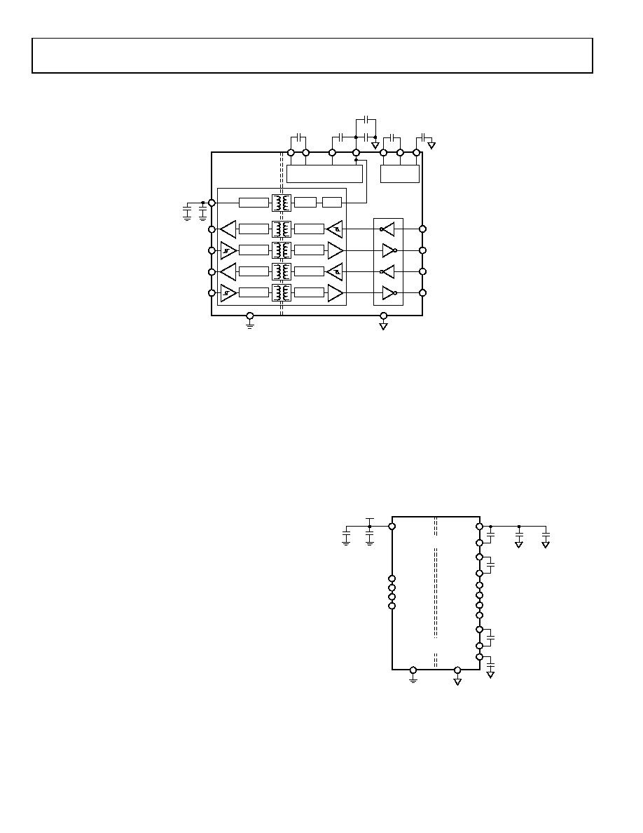
THEORY OF OPERATION
Figure 15. Functional Block Diagram
The ADM3252E is a high speed, 2.5 kV, fully isolated, dual-
channel RS-232 transceiver device that operates from a single
power supply.
The internal circuitry consists of the following main sections:
Isolation of power and data
Charge pump voltage converter
3.3 V logic to EIA/TIA-232E transmitter
EIA/TIA-232E to 3.3 V logic receiver
ISOLATION OF POWER AND DATA
The ADM3252E incorporates a dc-to-dc converter section,
which works on principles that are common to most power
supply designs. VCC power is supplied to an oscillating circuit
that switches current into a chip scale air core transformer. Power
is transferred to the secondary side where it is rectified to a high
dc voltage. The power is then linearly regulated to 3.3 V and
supplied to the secondary side data section and to the VISO pin.
Because the oscillator runs at a constant high frequency
independent of the load, excess power is internally dissipated
in the output voltage regulation process. Limited space for
transformer coils and components adds to the internal power
dissipation. This results in low power conversion efficiency.
The transmitter input (TINx) accepts TTL/CMOS input levels.
The driver input signal that is applied to the TINx pins is
referenced to logic ground (GND). It is coupled across the
isolation barrier, inverted, and then appears at the transceiver
section, referenced to isolated ground (GNDISO).
Similarly, the receiver input (RINx) accepts RS-232 signal levels
referenced to isolated ground (GNDISO). The RINx input is
inverted and coupled across the isolation barrier to appear at
the ROUTx pin, referenced to logic ground (GND).
The digital signals are transmitted across the isolation barrier
using iCoupler technology. Chip scale transformer windings
couple the digital signals magnetically from one side of the
barrier to the other. Digital inputs are encoded into waveforms
that are capable of exciting the primary transformer of the winding.
At the secondary winding, the induced waveforms are decoded
into the binary value that was originally transmitted.
Figure 16. Typical Operating Circuit
RECT
REG
V–
C4
0.1F
16V
VOLTAGE
DOUBLER
C1+ C1– V+
VISO
C2+ C2–
VOLTAGE
INVERTER
VCC
GND
GNDISO
ADM3252E
OSC
DECODE
R
ROUT1
RIN1*
ENCODE
TIN1
T
TOUT1
ENCODE
DECODE
R
ROUT2
RIN2*
ENCODE
TIN2
T
TOUT2
ENCODE
DECODE
10
F
0.
1
F
C3
0.1F
10V
C2
0.1F
16V
0.1F
10F
C1
0.1F
16V
*INTERNAL 5k PULL-DOWN RESISTOR ON THE RS-232 INPUTS.
10
515-
0
03
+
C3
0.1F
10V
+ C1
0.1F
16V
+ C2
0.1F
16V
0.1F
+
C4
0.1F
16V
VISO
V+
C1+
C1–
EIA/TIA-232E OUTPUT
TOUT1
EIA/TIA-232E INPUT
RIN1
EIA/TIA-232E OUTPUT
TOUT2
EIA/TIA-232E INPUT
RIN2
C2+
C2–
V–
GNDISO
ISOLATION
BARRIER
CMOS OUTPUT
ROUT1
CMOS OUTPUT
ROUT2
CMOS INPUT
TIN1
CMOS INPUT
TIN2
GND
3.0V TO 5.5V
VCC
0.1F
10F
ADM3252E
10F
10
51
5-
0
04
相关PDF资料 |
PDF描述 |
|---|---|
| M3DDA-2036R | IDC CABLE - MKR20A/MC20M/MKR20A |
| M3BBA-2036R | IDC CABLE - MSR20A/MC20M/MSR20A |
| V300C3V3T50BF3 | CONVERTER MOD DC/DC 3.3V 50W |
| V300C36T75BL2 | CONVERTER MOD DC/DC 36V 75W |
| GCM25DCCD-S189 | CONN EDGECARD 50POS R/A .156 SLD |
相关代理商/技术参数 |
参数描述 |
|---|---|
| EVAL-ADM4168EEBZ | 功能描述:界面开发工具 EVALUATION BOARD RoHS:否 制造商:Bourns 产品:Evaluation Boards 类型:RS-485 工具用于评估:ADM3485E 接口类型:RS-485 工作电源电压:3.3 V |
| EVAL-ADM8830EB | 制造商:Analog Devices 功能描述:EVALUATION BOARD I.C. - Bulk |
| EVAL-ADM8843EB | 制造商:Analog Devices 功能描述:EVALUATION BOARD I.C. - Bulk |
| EVAL-ADM8845EB | 制造商:AD 制造商全称:Analog Devices 功能描述:Charge Pump Driver for LCD White LED Backlights |
| EVAL-ADMP401-1Z | 制造商:Analog Devices 功能描述:EB OMNI DIRECTIONAL MICROPHONE - ANALOG - Boxed Product (Development Kits) |
发布紧急采购,3分钟左右您将得到回复。