- 您现在的位置:买卖IC网 > PDF目录17112 > EVAL-ADUC7028QSZ (Analog Devices Inc)KIT DEV ADUC7028 QUICK START PDF资料下载
参数资料
| 型号: | EVAL-ADUC7028QSZ |
| 厂商: | Analog Devices Inc |
| 文件页数: | 51/104页 |
| 文件大小: | 0K |
| 描述: | KIT DEV ADUC7028 QUICK START |
| 产品培训模块: | ARM7 Applications & Tools Intro to ARM7 Core & Microconverters Process Control |
| 标准包装: | 1 |
| 系列: | QuickStart™ 套件 |
| 类型: | MCU |
| 适用于相关产品: | ADuC7028 |
| 所含物品: | 评估板、电源、缆线、软件和说明文档 |
| 产品目录页面: | 739 (CN2011-ZH PDF) |
| 相关产品: | ADUC7028BBCZ62-RL-ND - IC MCU FLASH 62K 12BIT ADUC7028BBCZ62-ND - IC MCU FLASH 62K 12BIT |
第1页第2页第3页第4页第5页第6页第7页第8页第9页第10页第11页第12页第13页第14页第15页第16页第17页第18页第19页第20页第21页第22页第23页第24页第25页第26页第27页第28页第29页第30页第31页第32页第33页第34页第35页第36页第37页第38页第39页第40页第41页第42页第43页第44页第45页第46页第47页第48页第49页第50页当前第51页第52页第53页第54页第55页第56页第57页第58页第59页第60页第61页第62页第63页第64页第65页第66页第67页第68页第69页第70页第71页第72页第73页第74页第75页第76页第77页第78页第79页第80页第81页第82页第83页第84页第85页第86页第87页第88页第89页第90页第91页第92页第93页第94页第95页第96页第97页第98页第99页第100页第101页第102页第103页第104页
ADuC7019/20/21/22/24/25/26/27/28/29
Data Sheet
Rev. F | Page 50 of 104
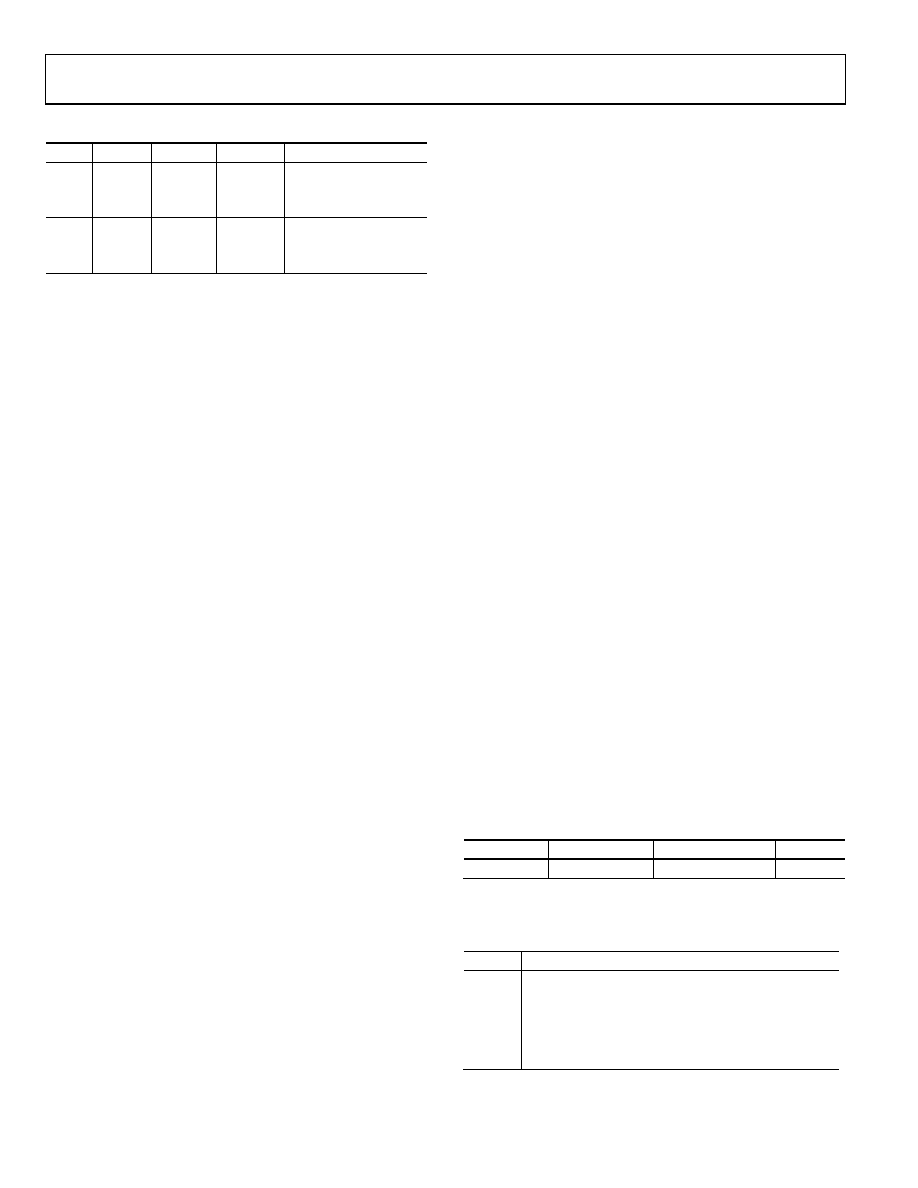
Table 28. VCM Ranges
AVDD
VREF
VCM Min
VCM Max
Signal Peak-to-Peak
3.3 V
2.5 V
1.25 V
2.05 V
2.5 V
2.048 V
1.024 V
2.276 V
2.048 V
1.25 V
0.75 V
2.55 V
1.25 V
3.0 V
2.5 V
1.25 V
1.75 V
2.5 V
2.048 V
1.024 V
1.976 V
2.048 V
1.25 V
0.75 V
2.25 V
1.25 V
CALIBRATION
By default, the factory-set values written to the ADC offset
(ADCOF) and gain coefficient registers (ADCGN) yield
optimum performance in terms of end-point errors and
linearity for standalone operation of the part (see the
Specifications section). If system calibration is required, it is
possible to modify the default offset and gain coefficients to
improve end-point errors, but note that any modification to the
factory-set ADCOF and ADCGN values can degrade ADC
linearity performance.
For system offset error correction, the ADC channel input stage
must be tied to AGND. A continuous software ADC conversion
loop must be implemented by modifying the value in ADCOF until
the ADC result (ADCDAT) reads Code 0 to Code 1. If the
ADCDAT value is greater than 1, ADCOF should be decremented
until ADCDAT reads 0 to 1. Offset error correction is done
digitally and has a resolution of 0.25 LSB and a range of
±3.125% of VREF.
For system gain error correction, the ADC channel input stage
must be tied to VREF. A continuous software ADC conversion
loop must be implemented to modify the value in ADCGN
until the ADC result (ADCDAT) reads Code 4094 to Code 4095.
If the ADCDAT value is less than 4094, ADCGN should be
incremented until ADCDAT reads 4094 to 4095. Similar to the
offset calibration, the gain calibration resolution is 0.25 LSB
with a range of ±3% of VREF.
TEMPERATURE SENSOR
The ADuC7019/20/21/22/24/25/26/27/28/29 provide voltage
output from on-chip band gap references proportional to
absolute temperature. This voltage output can also be routed
through the front-end ADC multiplexer (effectively an additional
ADC channel input) facilitating an internal temperature sensor
channel, measuring die temperature to an accuracy of ±3°C.
The following is an example routine showing how to use the
internal temperature sensor:
int main(void)
{
float a = 0;
short b;
ADCCON = 0x20;
// power-on the ADC
delay(2000);
ADCCP = 0x10;
// Select Temperature
Sensor as an // input to the ADC
REFCON = 0x01; // connect internal 2.5V
reference // to Vref pin
ADCCON = 0xE4; // continuous conversion
while(1)
{
while (!ADCSTA){};
// wait for end of conversion
b = (ADCDAT >> 16);
// To calculate temperature in °C, use
the formula:
a = 0x525 - b;
// ((Temperature = 0x525 - Sensor
Voltage) / 1.3)
a /= 1.3;
b = floor(a);
printf("Temperature: %d
oC\n",b);
}
return 0;
}
BAND GAP REFERENCE
Each ADuC7019/20/21/22/24/25/26/27/28/29 provides an on-
chip band gap reference of 2.5 V, which can be used for the ADC
and DAC. This internal reference also appears on the VREF pin.
When using the internal reference, a 0.47 F capacitor must be
connected from the external VREF pin to AGND to ensure stability
and fast response during ADC conversions. This reference can
also be connected to an external pin (VREF) and used as a refer-
ence for other circuits in the system. An external buffer is required
because of the low drive capability of the VREF output. A program-
mable option also allows an external reference input on the VREF
pin. Note that it is not possible to disable the internal reference.
Therefore, the external reference source must be capable of
overdriving the internal reference source.
Table 29. REFCON Register
Name
Address
Default Value
Access
REFCON
0xFFFF048C
0x00
R/W
The band gap reference interface consists of an 8-bit MMR
REFCON, described in Table 30.
Table 30. REFCON MMR Bit Designations
Bit
Description
7:1
Reserved.
0
Internal reference output enable. Set by user to
connect the internal 2.5 V reference to the VREF pin.
The reference can be used for an external component
but must be buffered. Cleared by user to disconnect
the reference from the VREF pin.
相关PDF资料 |
PDF描述 |
|---|---|
| GMM12DREN | CONN EDGECARD 24POS .156 EYELET |
| GSM12DREH | CONN EDGECARD 24POS .156 EYELET |
| EA-XPR-001 | BOARD LPCXPRESSO LPC1343 |
| EVAL-ADUC841QSZ | KIT DEV FOR ADUC841 QUICK START |
| HBM11DRAI | CONN EDGECARD 22POS R/A .156 SLD |
相关代理商/技术参数 |
参数描述 |
|---|---|
| EVAL-ADUC7029QSZ | 功能描述:EVAL DEV SYSTEM FOR ADUC7029 RoHS:否 类别:编程器,开发系统 >> 通用嵌入式开发板和套件(MCU、DSP、FPGA、CPLD等) 系列:* 标准包装:1 系列:PICDEM™ 类型:MCU 适用于相关产品:PIC10F206,PIC16F690,PIC16F819 所含物品:板,线缆,元件,CD,PICkit 编程器 产品目录页面:659 (CN2011-ZH PDF) |
| EVAL-ADUC7029QSZ | 制造商:Analog Devices 功能描述:Silicon Manufacturer:Analog Devices C |
| EVAL-ADUC7032QSPZ | 制造商:Analog Devices 功能描述:EVAL BD FOR ADUC7032 - Bulk |
| EVAL-ADUC7033QSPZ | 制造商:Analog Devices 功能描述:QUICK START DEVELOPMENT SYSTEM - Bulk |
| EVAL-ADUC7034QSPZ | 制造商:Analog Devices 功能描述:EVALUATION BOARD - Boxed Product (Development Kits) |
发布紧急采购,3分钟左右您将得到回复。