- 您现在的位置:买卖IC网 > PDF目录16543 > EVAL-ADV7180-32EBZ (Analog Devices Inc)BOARD EVAL FOR ADV7180 PDF资料下载
参数资料
| 型号: | EVAL-ADV7180-32EBZ |
| 厂商: | Analog Devices Inc |
| 文件页数: | 10/116页 |
| 文件大小: | 0K |
| 描述: | BOARD EVAL FOR ADV7180 |
| 标准包装: | 1 |
| 系列: | Advantiv® |
| 主要目的: | 视频,SDTV 视频解码器 - NTSC,PAL,SECAM |
| 嵌入式: | 否 |
| 已用 IC / 零件: | ADV7180 |
| 主要属性: | CVBS(复合),Y/C(S 视频)和 YPrPb(元件)输入 |
| 次要属性: | 8 位 ITU-R BT.656 YCrCb 4:2:2 输出 |
| 已供物品: | 板 |
第1页第2页第3页第4页第5页第6页第7页第8页第9页当前第10页第11页第12页第13页第14页第15页第16页第17页第18页第19页第20页第21页第22页第23页第24页第25页第26页第27页第28页第29页第30页第31页第32页第33页第34页第35页第36页第37页第38页第39页第40页第41页第42页第43页第44页第45页第46页第47页第48页第49页第50页第51页第52页第53页第54页第55页第56页第57页第58页第59页第60页第61页第62页第63页第64页第65页第66页第67页第68页第69页第70页第71页第72页第73页第74页第75页第76页第77页第78页第79页第80页第81页第82页第83页第84页第85页第86页第87页第88页第89页第90页第91页第92页第93页第94页第95页第96页第97页第98页第99页第100页第101页第102页第103页第104页第105页第106页第107页第108页第109页第110页第111页第112页第113页第114页第115页第116页
Data Sheet
ADV7180
Rev. I | Page 107 of 116
PCB LAYOUT RECOMMENDATIONS
The ADV7180 is a high precision, high speed, mixed-signal
device. To achieve the maximum performance from the part, it
is important to have a well laid out PCB. The following is a
guide for designing a board using the ADV7180.
ANALOG INTERFACE INPUTS
Take care when routing the inputs on the PCB. Keep track
lengths to a minimum, and use 75 trace impedances when
possible. In addition, trace impedances other than 75
increase the chance of reflections.
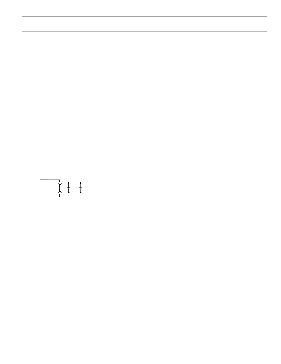
POWER SUPPLY DECOUPLING
It is recommended to decouple each power supply pin with
0.1 F and 10 nF capacitors. The fundamental idea is to have a
decoupling capacitor within about 0.5 cm of each power pin. In
addition, avoid placing the capacitor on the opposite side of the
PCB from the ADV7180 because doing so interposes inductive
vias in the path. The decoupling capacitors must be located
between the power plane and the power pin. Current must flow
from the power plane to the capacitor and then to the power
pin. Do not apply the power connection between the capacitor
and the power pin. Placing a via underneath the 100 nF
capacitor pads, down to the power plane, is the best approach
05700-
046
SUPPLY
GROUND
10nF
100nF
VIA TO SUPPLY
VIA TO GND
Figure 56. Recommended Power Supply Decoupling
It is particularly important to maintain low noise and good
stability of PVDD. Careful attention must be paid to regulation,
filtering, and decoupling. It is highly desirable to provide separate
regulated supplies for each of the analog circuitry groups (AVDD,
DVDD, DVDDIO, and PVDD).
Some graphic controllers use substantially different levels of
power when active (during active picture time) and when idle
(during horizontal and vertical sync periods). This can result in
a measurable change in the voltage supplied to the analog supply
regulator, which can in turn produce changes in the regulated
analog supply voltage. This can be mitigated by regulating the
analog supply, or at least PVDD, from a different, cleaner power
source, for example, from a 12 V supply.
Using a single ground plane for the entire board is also recom-
mended.
Experience repeatedly shows that the noise performance is the
same or better with a single ground plane. Using multiple ground
planes can be detrimental because each separate ground plane is
smaller, and long ground loops can result.
PLL
Place the PLL loop filter components as close as possible to the
ELPF pin. It must also be placed on the same side of the PCB as
the ADV7180. Do not place any digital or other high frequency
traces near these components. Use the values suggested in this
data sheet with tolerances of 10% or less.
VREFN AND VREFP
Place the circuit associated with these pins as close as possible
and on the same side of the PCB as the ADV7180.
DIGITAL OUTPUTS (BOTH DATA AND CLOCKS)
Try to minimize the trace length that the digital outputs have to
drive. Longer traces have higher capacitance, requiring more
current and, in turn, causing more internal digital noise.
Shorter traces reduce the possibility of reflections.
Adding a 30 to 50 series resistor can suppress reflections,
reduce EMI, and reduce the current spikes inside the ADV7180.
If series resistors are used, place them as close as possible to the
ADV7180 pins. However, try not to add vias or extra length to
the output trace to place the resistors closer.
If possible, limit the capacitance that each of the digital outputs
drives to less than 15 pF. This can easily be accomplished by
keeping traces short and by connecting the outputs to only one
device. Loading the outputs with excessive capacitance increases
the current transients inside the ADV7180, creating more digital
noise on its power supplies.
The 40-lead and 32-lead LFCSP have an exposed metal paddle
on the bottom of the package. This paddle must be soldered to
PCB ground for proper heat dissipation and for noise and
mechanical strength benefits.
DIGITAL INPUTS
The digital inputs on the ADV7180 are designed to work with
1.8 V to 3.3 V signals and are not tolerant of 5 V signals. Extra
components are needed if 5 V logic signals are required to be
applied to the decoder.
相关PDF资料 |
PDF描述 |
|---|---|
| M1DXK-2436J | IDC CABLE - MKR24K/MC24G/X |
| AD818AR-EBZ | BOARD EVAL FOR AD818AR |
| 5504970-2 | CABLE ASSEM FIBER SC-SC 2 METER |
| AD817AR-EBZ | BOARD EVAL FOR AD817AR |
| AD813AR-14-EBZ | BOARD EVAL FOR AD813AR-14 |
相关代理商/技术参数 |
参数描述 |
|---|---|
| EVAL-ADV7180-48EBZ | 制造商:AD 制造商全称:Analog Devices 功能描述:10-Bit, 4?? Oversampling SDTV Video Decoder |
| EVAL-ADV7180-48EBZ-8P-CAL | 制造商:Analog Devices 功能描述: |
| EVAL-ADV7180LFEB | 制造商:Analog Devices 功能描述:ADV7180 EVAL BOARD - Bulk |
| EVAL-ADV7180LFEBZ | 功能描述:BOARD EVAL FOR ADV7180 LFCSP RoHS:是 类别:编程器,开发系统 >> 评估演示板和套件 系列:Advantiv® 标准包装:1 系列:PSoC® 主要目的:电源管理,热管理 嵌入式:- 已用 IC / 零件:- 主要属性:- 次要属性:- 已供物品:板,CD,电源 |
| EVAL-ADV7180LQEBZ | 功能描述:BOARD EVALUATION ADV7180 RoHS:是 类别:编程器,开发系统 >> 评估演示板和套件 系列:Advantiv® 标准包装:1 系列:- 主要目的:电信,线路接口单元(LIU) 嵌入式:- 已用 IC / 零件:IDT82V2081 主要属性:T1/J1/E1 LIU 次要属性:- 已供物品:板,电源,线缆,CD 其它名称:82EBV2081 |
发布紧急采购,3分钟左右您将得到回复。