- 您现在的位置:买卖IC网 > PDF目录93448 > EVB71102 EVB71102 EValuation Board for TH71102 Receiver PDF资料下载
参数资料
| 型号: | EVB71102 |
| 英文描述: | EVB71102 EValuation Board for TH71102 Receiver |
| 中文描述: | EVB71102评估板接收机TH71102 |
| 文件页数: | 2/8页 |
| 文件大小: | 211K |
| 代理商: | EVB71102 |
EVB71071
315/433MHz Transmitter
Evaluation Board Description
390127107101
2 of 8
EVB Description
Rev. 003
Aug/02
Theory of Operation
General
As depicted in Fig.1, the TH71071 transmitter
consists of a fully integrated voltage-controlled
oscillator (VCO), a divide-by-32 divider (div32), a
phase-frequency detector (PFD) and a charge
pump. An external loop filter at pin LF determines
the dynamic behaviour of the PLL and suppresses
reference spurious signals.
The VCO’s output signal feeds the power amplifier
(PA). RF signal power Po can be adjusted in six
steps from Po = –12 dBm to +2 dBm either by
changing the value of resistor R1 or by varying the
voltage VPS at pin PS/DATA. The open-collector
differential output (OUT1, OUT2) can be used to
either directly drive a loop antenna or to be
converted to a single-ended impedance by means
of a balanced-to-unbalanced (balun) transformer.
For
maximum
available
output
power,
the
differential output should be matched to a load of
approx. 1 k
.
Bandgap biasing ensures stable operation of the IC
at a power supply range of 2.2 V to 5.5 V.
ASK Modulation
The TH71071 can be ASK-modulated by applying
data directly at pin PS. This turns the PA on and off
and therefore leads to an ASK signal at the output.
LO Source
Many applications require a stable RF source. For
this purpose, the TH71071 can be used without
modulation
as
an
easy-to-use,
PLL-stabilized,
continuous wave (CW) generator.
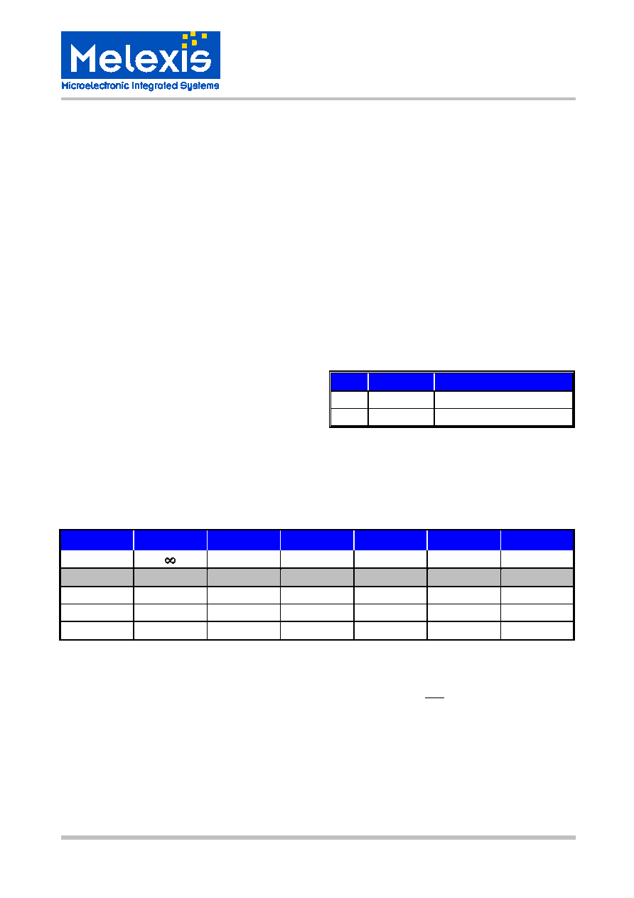
Mode Control Logic
The mode control logic allows two different modes
of operation as listed in the following table. The
mode control pin ENTX is pulled-down internally.
This guarantees that the whole circuit is shut down
if this pin is left floating.
ENTX
Mode
Description
0
TX disabled whole circuit in standby
1
TX enable
TX active
Table 1: Modes of operation
Output Power Selection
typical values at Ta = 23 °C and Vcc = 3 V:
R1 / k
0
7.5
11
15
24
43
R2 / k
4.7
VPS / V
≥≥≥≥ 2
1.1
0.9
0.7
0.5
0.3
Icc / mA
11.5
8.6
7.3
6.2
5.3
4.8
Po / dBm
2
-1
-4
-7
-10
-12
Pharm / dBm
≤-40
≤-45
≤-50
Table 2: Output Power Selection
If the transmitter is operated at any supply voltage Vcc,
the values for R1 and R2 can be calculated as allows:
=
1
2
1
PS
cc
V
R
For more detailed information, please refer to the latest TH71071 data sheet revision.
.
相关PDF资料 |
PDF描述 |
|---|---|
| EVB71111 | EVB71111 EValuation Board for TH71111 Receiver |
| EVB71112 | EVB71112 EValuation Board for TH71112 Receiver |
| EVB7120 | EVB7120 EValuation Board For TH7120 300 to 930MHz FSK/FM/ASK Transceiver |
| EVB90255 | EVB90255 EValuation Board for the MLX90255 |
| EVB90601 | EVB90601 EValuation Board for the MLX90601 |
相关代理商/技术参数 |
参数描述 |
|---|---|
| EVB71102-315-ASK-A | 制造商:MELEXIS 制造商全称:Melexis Microelectronic Systems 功能描述:315/433MHz Receiver Evaluation Board Description |
| EVB71102-315-ASK-C | 制造商:MELEXIS 制造商全称:Melexis Microelectronic Systems 功能描述:315/433MHz Receiver Evaluation Board Description |
| EVB71102-315-FM-A | 制造商:MELEXIS 制造商全称:Melexis Microelectronic Systems 功能描述:315/433MHz Receiver Evaluation Board Description |
| EVB71102-315-FM-C | 制造商:MELEXIS 制造商全称:Melexis Microelectronic Systems 功能描述:315/433MHz Receiver Evaluation Board Description |
| EVB71102-315-FSK-A | 制造商:MELEXIS 制造商全称:Melexis Microelectronic Systems 功能描述:315/433MHz Receiver Evaluation Board Description |
发布紧急采购,3分钟左右您将得到回复。