- 您现在的位置:买卖IC网 > PDF目录93448 > EVB90601 EVB90601 EValuation Board for the MLX90601 PDF资料下载
参数资料
| 型号: | EVB90601 |
| 英文描述: | EVB90601 EValuation Board for the MLX90601 |
| 中文描述: | EVB90601评估板MLX90601 |
| 文件页数: | 3/5页 |
| 文件大小: | 125K |
| 代理商: | EVB90601 |
MLX90255
Linear Optical Array
MLX90255 Linear Optical Array
Page 3 of 5
Rev 1.0 31-May-01
appropriate SI pulse to the optical array. The
required pull-down resistors are also foreseen
on the board. All important signals (SI, CLK,
VOUT, 5V and GND) are connected to test
terminals, which makes it easy to visualize them
on an oscilloscope. One sensor in a SMD
package is soldered on the PCB (called B) while
an external sensor can be connected to the 5-
pins connector row (upper right corner) (called
A). Both output signals are connected to test
terminals,
called
respectively
VOUTB
and
VOUTA.
An external regulated DC power supply, with an
output voltage between 6 and 10V, needs to be
connected to the screw connector in the upper
left corner of the PCB. A regular 9V battery is
also possible. (Mind the sign!) As soon as the
power supply is switched on, a LED lights up
and the micro controller starts generating the
CLK and SI signals with the selected frequency
and integration time.
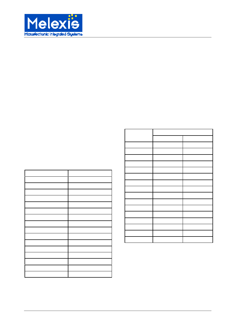
The frequency of the signal CLK can be chosen
with the rotary DIL switch on the right. The
frequencies corresponding to the 16 positions of
this switch are shown in the following table.
Position
CLK frequency
0
36kHz
1
64kHz
2
77kHz
3
93kHz
4
112kHz
5
141kHz
6
170kHz
7
214kHz
8
284kHz
9
345kHz
A
435kHz
B
588kHz
C
909kHz
D
1.0MHz
E
1.25MHz
F
1.67MHz
Positions 0, E and F correspond to frequencies
that are outside the device specification. Lighting
up a second LED indicates selecting one of
them.
For
each
SI
pulse,
133
CLK
pulses
are
generated with the selected frequency, and after
them the CLK line is pulled low until the next SI
pulse. See further in this document for the
correct timings.
The light integration time can be selected with
the other rotary DIL switch. Again 16 positions
are possible, however now there is no one-to-
one relation with the corresponding integration
times. Actually the switch specifies a time which
starts only after the 133
rd CLK pulse. As the
integration time already starts after the 18
th pulse
(see device specification), the total integration
time also depends on the selected frequency.
The following table shows for each position (of
the ‘integration time switch’) the minimal and the
maximal
integration
time,
corresponding
to
respectively the maximal and the minimal CLK
frequency.
Total Integration Time
Position
Minimal
Maximal
0
79us
3.17ms
1
230us
3.33ms
2
380us
3.48ms
3
682us
3.77ms
4
985us
4.09ms
5
1.30ms
4.40ms
6
2.50ms
5.60ms
7
3.10ms
6.20ms
8
3.85ms
6.95ms
9
4.60ms
7.70ms
A
6.10ms
9.15ms
B
7.7ms
10.7s
C
9.15ms
12.5ms
D
10.5ms
E
15ms
F
20ms
The analog output voltage is directly proportional
to the light intensity and the integration time up
to the devices saturation level (3V typical). The
response of a pixel can be described with the
following formula:
VOUT = PR*Plight + offset + PRerror*Plight + DC
where DC means the dark current.
The
proportionality
constant
PR
is
the
responsivity
of
the
device
given
in
(V*cm2/W*sec).
Responsivity
is
wavelength
相关PDF资料 |
PDF描述 |
|---|---|
| EVK75-050 | TRANSISTOR | BJT POWER MODULE | HALF BRIDGE | DARLINGTON | 600V V(BR)CEO | 75A I(C) |
| EVS100K | ARAMIS Image Sensor Chip |
| EVS1010 | Consumer IC |
| EVS1410 | Consumer IC |
| EVS250K | ARAMIS Image Sensor Chip |
相关代理商/技术参数 |
参数描述 |
|---|---|
| EVB90609L-N2 | 制造商:Melexis Semiconductors 功能描述:EVALUATION BOARD FOR MLX90609-N2 |
| EVB90614 | 功能描述:BOARD EVAL FOR MLX90614 RoHS:是 类别:编程器,开发系统 >> 评估板 - 传感器 系列:- 产品培训模块:Lead (SnPb) Finish for COTS Obsolescence Mitigation Program 标准包装:1 系列:- |
| EVB90615 | 功能描述:EVAL BOARD FOR MLX90615 RoHS:否 类别:编程器,开发系统 >> 评估板 - 传感器 系列:- 产品培训模块:Lead (SnPb) Finish for COTS Obsolescence Mitigation Program 标准包装:1 系列:- |
| EVB90620 | 制造商:Melexis Semiconductors 功能描述:BOARD EVALUATION FOR MLX90620 制造商:Melexis Semiconductors 功能描述:Evaluation Board for MLX90620 Temperature Array |
| EVB9118-MINI | 功能描述:BOARD EVAL FOR LAN9118 MINI CARD RoHS:是 类别:编程器,开发系统 >> 过时/停产零件编号 系列:- 标准包装:1 系列:- 传感器类型:CMOS 成像,彩色(RGB) 传感范围:WVGA 接口:I²C 灵敏度:60 fps 电源电压:5.7 V ~ 6.3 V 嵌入式:否 已供物品:成像器板 已用 IC / 零件:KAC-00401 相关产品:4H2099-ND - SENSOR IMAGE WVGA COLOR 48-PQFP4H2094-ND - SENSOR IMAGE WVGA MONO 48-PQFP |
发布紧急采购,3分钟左右您将得到回复。