- 您现在的位置:买卖IC网 > PDF目录370147 > FAN5242QSC PDF资料下载
参数资料
| 型号: | FAN5242QSC |
| 文件页数: | 3/20页 |
| 文件大小: | 123K |
| 代理商: | FAN5242QSC |
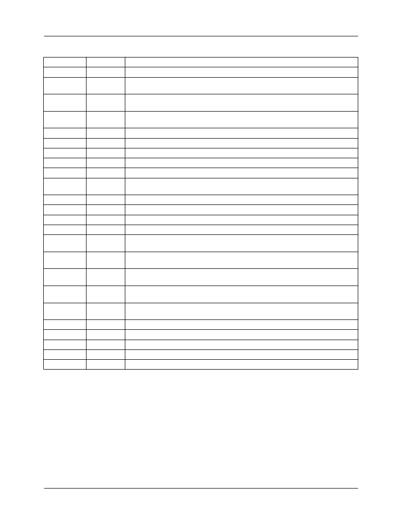
FAN5201
3
P
Pin Descriptions
Pin Number
1
2
Pin Name
SDA
IFB
Pin Function Description
Serial Data
. SMBus data I/O.
Current Feedback.
a battery current sense resistor.
Voltage Feedback.
terminals.
Battery.
Output current sense -. Connect this pin to the negative side of a battery
current sense resistor.
Current Compensation.
Frequency compensation for current loop.
Voltage Compensation.
Frequency compensation for voltage loop.
5V Digital Input.
5V internal power.
5V Analog Input.
Connect to 5V power. See Figure 4.
Drive.
Base (gate) drive for external PNP (P-channel MOSFET).
Power Supply.
Power source node, powered either by the AC adapter or by the
battery.
Low Side FET Driver.
Drive for low side switching MOSFET Q4.
Power Ground.
High Side FET Driver.
Drive for high side switching MOSFET Q3.
DC Power Input.
Connect to the AC adapter input.
Soft Start and Current Limit.
Connect to an external MOSFET for limiting inrush
and fault current.
Input Power Sense +.
Connect this pin to the positive side of an adapter current
sense resistor.
Input Power Sense -.
Connect this pin to the negative side of an adapter current
sense resistor.
Input Isolation Drive.
Q2 gate drive. Attach to a P-channel MOSFET to prevent
battery backfeed.
Signal Ground.
Attach all small signal grounds to this pin, and attach the pin to the
ground plane with a single connection.
Power Compensation.
Frequency compensation for power loop.
Soft Start.
Connect to a capacitor to softstart.
Voltage Threshold.
Sets the level at which ACAV trips.
AC Available.
Open collector output signaling that the AC adapter is present.
Serial Clock.
SMBus clock input.
Output current sense +. Connect this pin to the positive side of
3
VFB
Voltage remote sense feedback. Connect this pin to the battery
4
BAT
5
6
7
8
9
CompI
CompV
DIG5V
AM5V
DRV
PSIN
10
11
12
13
14
15
LODRV
PGND
HIDRV
DCIN
SSIN/ILIM
16
PSIN+
17
PSIN-
18
INISO
19
SGND
20
21
22
23
24
CompP
SS
Vth
ACAV
SCL
相关PDF资料 |
PDF描述 |
|---|---|
| FAN5242QSCX | |
| FAN5201 | |
| FAN8005D2TF | Servo Motor Controller/Driver |
| FAN8007D | Servo/Spindle Motor Controller/Driver |
| FAN8007DTF | Servo/Spindle Motor Controller/Driver |
相关代理商/技术参数 |
参数描述 |
|---|---|
| FAN5242QSCX | 功能描述:开关变换器、稳压器与控制器 PWM Controller RoHS:否 制造商:Texas Instruments 输出电压:1.2 V to 10 V 输出电流:300 mA 输出功率: 输入电压:3 V to 17 V 开关频率:1 MHz 工作温度范围: 安装风格:SMD/SMT 封装 / 箱体:WSON-8 封装:Reel |
| FAN5250 | 制造商:FAIRCHILD 制造商全称:Fairchild Semiconductor 功能描述:Mobile Processor Core-Voltage Regulator |
| FAN5250_ADB3026B WAF | 制造商:Fairchild Semiconductor Corporation 功能描述: |
| FAN5250_AZB3026B WAF | 制造商:Fairchild Semiconductor Corporation 功能描述: |
| FAN5250QSC | 功能描述:DC/DC 开关控制器 DC/DC RoHS:否 制造商:Texas Instruments 输入电压:6 V to 100 V 开关频率: 输出电压:1.215 V to 80 V 输出电流:3.5 A 输出端数量:1 最大工作温度:+ 125 C 安装风格: 封装 / 箱体:CPAK |
发布紧急采购,3分钟左右您将得到回复。