- 您现在的位置:买卖IC网 > PDF目录18632 > FDC5612 (Fairchild Semiconductor)MOSFET N-CH 60V 4.3A SSOT-6 PDF资料下载
参数资料
| 型号: | FDC5612 |
| 厂商: | Fairchild Semiconductor |
| 文件页数: | 2/5页 |
| 文件大小: | 0K |
| 描述: | MOSFET N-CH 60V 4.3A SSOT-6 |
| 产品培训模块: | High Voltage Switches for Power Processing |
| 产品变化通告: | Mold Compound Change 08/April/2008 |
| 产品目录绘图: | MOSFET SuperSOT-6 |
| 标准包装: | 1 |
| 系列: | PowerTrench® |
| FET 型: | MOSFET N 通道,金属氧化物 |
| FET 特点: | 逻辑电平门 |
| 漏极至源极电压(Vdss): | 60V |
| 电流 - 连续漏极(Id) @ 25° C: | 4.3A |
| 开态Rds(最大)@ Id, Vgs @ 25° C: | 55 毫欧 @ 4.3A,10V |
| Id 时的 Vgs(th)(最大): | 4V @ 250µA |
| 闸电荷(Qg) @ Vgs: | 18nC @ 10V |
| 输入电容 (Ciss) @ Vds: | 650pF @ 25V |
| 功率 - 最大: | 800mW |
| 安装类型: | 表面贴装 |
| 封装/外壳: | SOT-23-6 细型,TSOT-23-6 |
| 供应商设备封装: | 6-SSOT |
| 包装: | 标准包装 |
| 产品目录页面: | 1602 (CN2011-ZH PDF) |
| 其它名称: | FDC5612DKR |
�� �
�
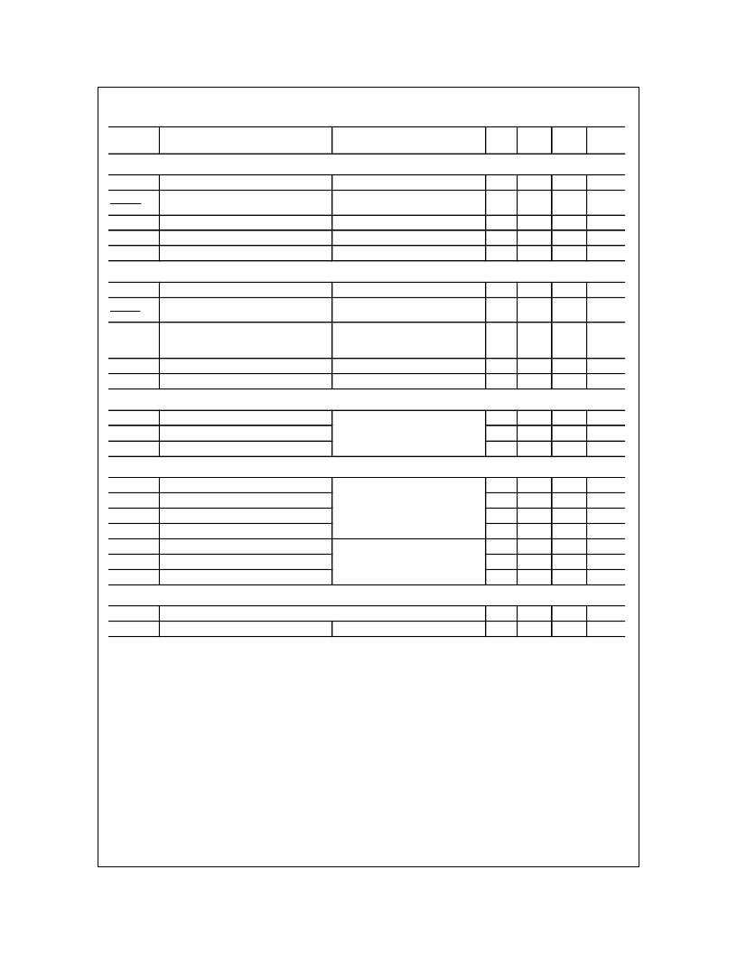
�Electrical� Characteristics�
�T� A� =� 25� °� C� unless� otherwise� noted�
�Symbol�
�Parameter�
�Test� Conditions�
�Min� Typ�
�Max� Units�
�Off� Characteristics�
�BV� DSS�
�?� BV� DSS�
�?� T� J�
�I� DSS�
�I� GSSF�
�I� GSSR�
�Drain-Source� Breakdown� Voltage�
�Breakdown� Voltage� Temperature�
�Coefficient�
�Zero� Gate� Voltage� Drain� Current�
�Gate-Body� Leakage� Current,� Forward�
�Gate-Body Leakage Current, Reverse�
�V� GS� =� 0� V,� I� D� =� 250� μ� A�
�I� D� =� 250� μ� A,� Referenced� to� 25� °� C�
�V� DS� =� 48� V,� V� GS� =� 0� V�
�V� GS� =� 20� V,� V� DS� =� 0� V�
�V� GS� =� -20� V,� V� DS� =� 0� V�
�60�
�58�
�1�
�100�
�-100�
�V�
�mV/� °� C�
�μ� A�
�nA�
�nA�
�On� Characteristics�
�(Note� 2)�
�V� GS(th)�
�?� V� GS(th)�
�?� T� J�
�R� DS(on)�
�Gate� Threshold� Voltage�
�Gate� Threshold� Voltage�
�Temperature� Coefficient�
�Static� Drain-Source�
�On-Resistance�
�V� DS� =� V� GS� ,� I� D� =� 250� μ� A�
�I� D� =� 250� μ� A,� Referenced� to� 25� °� C�
�V� GS� =� 10� V,� I� D� =� 4.3� A�
�V� GS� =� 10� V,� I� D� =� 4.3� A,� T� J� =� 125� °� C�
�2�
�2.2�
�-5.5�
�0.042�
�0.072�
�4�
�0.055�
�0.094�
�V�
�mV/� °� C�
�?�
�V� GS� =� 6� V,� I� D� =� 4� A�
�0.048�
�0.064�
�I� D(on)�
�g� FS�
�On-State� Drain� Current�
�Forward� Transconductance�
�V� GS� =� 10� V,� V� DS� =� 5� V�
�V� DS� =� 10� V,� I� D� =� 4.3� A�
�10�
�14�
�A�
�S�
�Dynamic� Characteristics�
�C� iss�
�C� oss�
�C� rss�
�Input� Capacitance�
�Output� Capacitance�
�Reverse� Transfer� Capacitance�
�V� DS� =� 25� V,� V� GS� =� 0� V,�
�f� =� 1.0� MHz�
�650�
�80�
�35�
�pF�
�pF�
�pF�
�Switching� Characteristics�
�(Note� 2)�
�t� d(on)�
�t� r�
�t� d(off)�
�t� f�
�Q� g�
�Q� gs�
�Q� gd�
�Turn-On� Delay� Time�
�Turn-On� Rise� Time�
�Turn-Off� Delay� Time�
�Turn-Off� Fall� Time�
�Total� Gate� Charge�
�Gate-Source� Charge�
�Gate-Drain� Charge�
�V� DD� =� 30� V,� I� D� =� 1� A,�
�V� GS� =� 10� V,� R� GEN� =� 6� ?�
�V� DS� =� 30� V,� I� D� =� 4.3� A,�
�V� GS� =� 10� V�
�11�
�8�
�19�
�6�
�12.5�
�2.4�
�2.6�
�20�
�18�
�35�
�15�
�18�
�ns�
�ns�
�ns�
�ns�
�nC�
�nC�
�nC�
�Drain-Source� Diode� Characteristics� and� Maximum� Ratings�
�I� S�
�Maximum� Continuous� Drain-Source� Diode� Forward� Current�
�1.3�
�A�
�V� SD�
�Drain-Source� Diode� Forward� Voltage�
�V� GS� =� 0� V,� I� S� =� 1.3� A�
�(Note� 2)�
�0.75�
�1.2�
�V�
�Notes:�
�1.� R� q� JA� is� the� sum� of� the� junction-to-case� and� case-to-ambient� resistance� where� the� case� thermal� reference� is� defined� as� the� solder� mounting� surface�
�of� the� drain� pins.� R� q� JC� is� guaranteed� by� design� while� R� q� CA� is� determined� by� the� user's� board� design.�
�a)� 78� °� C/W� when� mounted� on� a� 1.0� in� 2� pad� of� 2� oz.� copper.�
�b)� 156� °� C/W� when� mounted� on� a� minimum� pad.�
�2.� Pulse� Test:� Pulse� Width� £� 300� m� s,� Duty� Cycle� £� 2.0%�
�FDC5612� Rev.� C2�
�相关PDF资料 |
PDF描述 |
|---|---|
| 2N7002 | MOSFET N-CH 60V 115MA SOT-23 |
| MS-151/CF-MD | TOOL SLDR FIX FOR MS-151-C(LP) |
| 565P5P72 | CABLE STR MALE-MALE 5POS 6' |
| 553S3P144 | CBL STR FEMAL-R/A MALE 3POS 12' |
| DRD10E04 | SWITCH ROTARY DIP 10POS BCD SEAL |
相关代理商/技术参数 |
参数描述 |
|---|---|
| FDC5612 | 制造商:Fairchild Semiconductor Corporation 功能描述:MOSFET N SUPERSOT-6 |
| FDC5612_04 | 制造商:FAIRCHILD 制造商全称:Fairchild Semiconductor 功能描述:60V N-Channel PowerTrench㈢ MOSFET |
| FDC5612_F095 | 功能描述:MOSFET 60V 4.3A N-CH POWERTRENCH RoHS:否 制造商:STMicroelectronics 晶体管极性:N-Channel 汲极/源极击穿电压:650 V 闸/源击穿电压:25 V 漏极连续电流:130 A 电阻汲极/源极 RDS(导通):0.014 Ohms 配置:Single 最大工作温度: 安装风格:Through Hole 封装 / 箱体:Max247 封装:Tube |
| FDC5612NL | 制造商:Fairchild Semiconductor Corporation 功能描述:Trans MOSFET N-CH 60V 4.3A 6-Pin SuperSOT T/R |
| FDC5614 | 制造商:FAIRCHILD 制造商全称:Fairchild Semiconductor 功能描述:60V P-Channel Logic Level PowerTrench MOSFET |
发布紧急采购,3分钟左右您将得到回复。