- 您现在的位置:买卖IC网 > PDF目录375779 > FDP6670AS (FAIRCHILD SEMICONDUCTOR CORP) 30V N-Channel PowerTrench SyncFET PDF资料下载
参数资料
| 型号: | FDP6670AS |
| 厂商: | FAIRCHILD SEMICONDUCTOR CORP |
| 元件分类: | JFETs |
| 英文描述: | 30V N-Channel PowerTrench SyncFET |
| 中文描述: | 62 A, 30 V, 0.0085 ohm, N-CHANNEL, Si, POWER, MOSFET, TO-220AB |
| 封装: | TO-220, 3 PIN |
| 文件页数: | 2/5页 |
| 文件大小: | 156K |
| 代理商: | FDP6670AS |
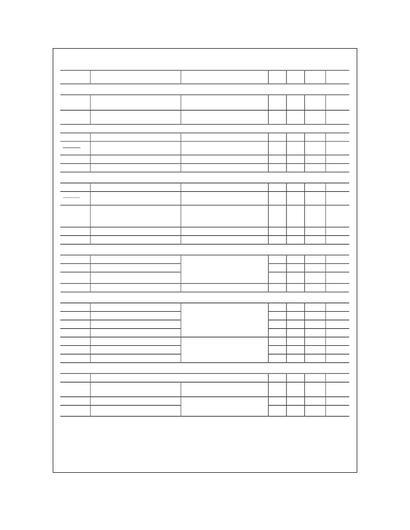
FDP6670AL/FDB6670AL Rev D(W)
Electrical Characteristics
T
A
= 25°C unless otherwise noted
Test Conditions
Symbol
Parameter
Min
Typ
Max
Units
Drain-Source Avalanche Ratings
(Note 1)
W
DSS
Single Pulse Drain-Source
Avalanche Energy
V
DD
= 15 V,
I
D
= 80 A
114
mJ
I
AR
Maximum Drain-Source Avalanche
Current
Off Characteristics
BV
DSS
Drain–Source Breakdown Voltage
BV
DSS
T
J
Coefficient
I
DSS
Zero Gate Voltage Drain Current
I
GSS
Gate–Body Leakage
80
A
V
GS
= 0 V,
I
D
= 250
μ
A, Referenced to 25
°
C
I
D
= 250
μ
A
30
V
Breakdown Voltage Temperature
24
mV/
°
C
V
DS
= 24 V,
V
GS
=
±
20 V,
V
GS
= 0 V
V
DS
= 0 V
1
μ
A
nA
±
100
On Characteristics
V
GS(th)
V
GS(th)
T
J
R
DS(on)
(Note 2)
Gate Threshold Voltage
Gate Threshold Voltage
Temperature Coefficient
Static Drain–Source On–
Resistance
V
DS
= V
GS
,
I
D
= 250
μ
A, Referenced to 25
°
C
I
D
= 250
μ
A
1
1.9
3
V
–5
mV/
°
C
V
GS
= 10 V,
V
GS
= 4.5 V,
V
GS
= 10 V, I
D
= 40 A, T
J
=125
°
C
V
GS
= 10 V,
V
DS
= 10 V
V
DS
= 10V,
I
D
= 40 A
I
D
= 40 A
I
D
= 37 A
5.2
6.5
7.2
6.5
8.5
9.7
m
I
D(on)
g
FS
On–State Drain Current
Forward Transconductance
80
A
S
115
Dynamic Characteristics
C
iss
Input Capacitance
C
oss
Output Capacitance
2440
580
pF
pF
C
rss
Reverse Transfer Capacitance
V
DS
= 15 V,
f = 1.0 MHz
V
GS
= 0 V,
250
pF
R
G
Gate Resistance
V
GS
= 15 mV, f = 1.0 MHz
1.4
Switching Characteristics
t
d(on)
Turn–On Delay Time
t
r
Turn–On Rise Time
t
d(off)
Turn–Off Delay Time
t
f
Turn–Off Fall Time
Q
g
Total Gate Charge
Q
gs
Gate–Source Charge
Q
gd
Gate–Drain Charge
(Note 2)
13
13
42
15
24
7
9
23
23
68
27
33
ns
ns
ns
ns
nC
nC
nC
V
DD
= 10V,
V
GS
= 10 V,
I
D
= 1 A,
R
GEN
= 6
V
DS
= 15 V,
V
GS
= 5 V
I
D
= 40 A,
Drain–Source Diode Characteristics and Maximum Ratings
I
S
Maximum Continuous Drain–Source Diode Forward Current
Drain–Source Diode Forward
Voltage
t
rr
Diode Reverse Recovery Time
Q
rr
Diode Reverse Recovery Charge
80
A
V
SD
V
GS
= 0 V,
I
S
= 40 A
(Note 1)
0.9
1.3
V
34
24
nS
nC
I
F
= 40 A,
d
iF
/d
t
= 100 A/μs
Notes:
1. Pulse Test: Pulse Width < 300
μ
s, Duty Cycle < 2.0%
F
相关PDF资料 |
PDF描述 |
|---|---|
| FDP6670AS_NL | 30V N-Channel PowerTrench SyncFET |
| FDP7030 | N-Channel Logic Level PowerTrenchTM MOSFET |
| FDP7030BL | N-Channel Logic Level PowerTrenchTM MOSFET |
| FDP7030L | N-Channel Logic Level Enhancement Mode Field Effect Transistor |
| FDP7045 | N-Channel Logic Level PowerTrench MOSFET |
相关代理商/技术参数 |
参数描述 |
|---|---|
| FDP6670AS_08 | 制造商:FAIRCHILD 制造商全称:Fairchild Semiconductor 功能描述:30V N-Channel PowerTrench㈢ SyncFET⑩ |
| FDP6670AS_NL | 制造商:FAIRCHILD 制造商全称:Fairchild Semiconductor 功能描述:30V N-Channel PowerTrench SyncFET |
| FDP6670S | 功能描述:MOSFET 30V N-Ch PowerTrench RoHS:否 制造商:STMicroelectronics 晶体管极性:N-Channel 汲极/源极击穿电压:650 V 闸/源击穿电压:25 V 漏极连续电流:130 A 电阻汲极/源极 RDS(导通):0.014 Ohms 配置:Single 最大工作温度: 安装风格:Through Hole 封装 / 箱体:Max247 封装:Tube |
| FDP6676 | 功能描述:MOSFET 30V N-Ch PowerTrench Logic Level RoHS:否 制造商:STMicroelectronics 晶体管极性:N-Channel 汲极/源极击穿电压:650 V 闸/源击穿电压:25 V 漏极连续电流:130 A 电阻汲极/源极 RDS(导通):0.014 Ohms 配置:Single 最大工作温度: 安装风格:Through Hole 封装 / 箱体:Max247 封装:Tube |
| FDP6676S | 功能描述:MOSFET 30V N-Ch PowerTrench RoHS:否 制造商:STMicroelectronics 晶体管极性:N-Channel 汲极/源极击穿电压:650 V 闸/源击穿电压:25 V 漏极连续电流:130 A 电阻汲极/源极 RDS(导通):0.014 Ohms 配置:Single 最大工作温度: 安装风格:Through Hole 封装 / 箱体:Max247 封装:Tube |
发布紧急采购,3分钟左右您将得到回复。