- 您现在的位置:买卖IC网 > PDF目录67504 > FM32276-GTR SPECIALTY CONSUMER CIRCUIT, PDSO14 PDF资料下载
参数资料
| 型号: | FM32276-GTR |
| 元件分类: | 消费家电 |
| 英文描述: | SPECIALTY CONSUMER CIRCUIT, PDSO14 |
| 封装: | GREEN, MS-012AB, SOIC-14 |
| 文件页数: | 3/21页 |
| 文件大小: | 417K |
| 代理商: | FM32276-GTR |
FM32278/276/274/272 - 5V I2C Companion
Rev. 3.1
July 2010
Page 11 of 21
Two-wire Interface
The FM3227x employs an industry standard two-
wire bus that is familiar to many users. This product
is unique since it incorporates two logical devices in
one chip. Each logical device can be accessed
individually. Although monolithic, it appears to the
system software to be two separate products. One is
a memory device. It has a Slave Address (Slave ID =
1010b) that operates the same as a stand-alone
memory device. The second device is a real-time
clock and processor companion which have a unique
Slave Address (Slave ID = 1101b).
By convention, any device that is sending data onto
the bus is the transmitter while the target device for
this data is the receiver. The device that is
controlling the bus is the master. The master is
responsible for generating the clock signal for all
operations. Any device on the bus that is being
controlled is a slave. The FM3227x is always a slave
device.
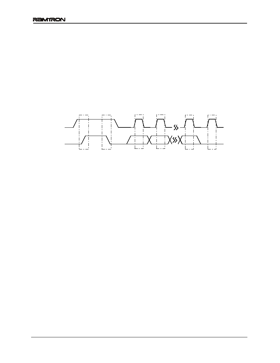
The bus protocol is controlled by transition states in
the SDA and SCL signals. There are four conditions:
Start, Stop, Data bit, and Acknowledge. The figure
below illustrates the signal conditions that specify
the four states. Detailed timing diagrams are shown
in the Electrical Specifications section.
Stop
(Master)
Start
(Master)
7
Data bits
(Transmitter)
6
0
Data bit
(Transmitter)
Acknowledge
(Receiver)
SCL
SDA
Figure 9. Data Transfer Protocol
Start Condition
A Start condition is indicated when the bus master
drives SDA from high to low while the SCL signal is
high. All read and write transactions begin with a
Start condition. An operation in progress can be
aborted by asserting a Start condition at any time.
Aborting an operation using the Start condition will
ready the FM3227x for a new operation.
If the power supply drops below the specified VTP
during operation, any 2-wire transaction in progress
will be aborted and the system must issue a Start
condition prior to performing another operation.
Stop Condition
A Stop condition is indicated when the bus master
drives SDA from low to high while the SCL signal is
high. All operations must end with a Stop condition.
If an operation is pending when a stop is asserted,
the operation will be aborted. The master must have
control of SDA (not a memory read) in order to
assert a Stop condition.
Data/Address Transfer
All data transfers (including addresses) take place
while the SCL signal is high. Except under the two
conditions described above, the SDA signal should
not change while SCL is high.
Acknowledge
The Acknowledge (ACK) takes place after the 8th
data bit has been transferred in any transaction.
During this state the transmitter must release the
SDA bus to allow the receiver to drive it. The
receiver drives the SDA signal low to acknowledge
receipt of the byte. If the receiver does not drive
SDA low, the condition is a No-Acknowledge
(NACK) and the operation is aborted.
The receiver might NACK for two distinct reasons.
First is that a byte transfer fails. In this case, the
NACK ends the current operation so that the part can
be addressed again. This allows the last byte to be
recovered in the event of a communication error.
Second and most common, the receiver does not
send an ACK to deliberately terminate an operation.
For example, during a read operation, the FM3227x
will continue to place data onto the bus as long as the
receiver sends ACKs (and clocks). When a read
operation is complete and no more data is needed,
the receiver must NACK the last byte. If the receiver
ACKs the last byte, this will cause the FM3227x to
attempt to drive the bus on the next clock while the
master is sending a new command such as a Stop.
相关PDF资料 |
PDF描述 |
|---|---|
| FM32276-G | SPECIALTY CONSUMER CIRCUIT, PDSO14 |
| FM32278-GTR | SPECIALTY CONSUMER CIRCUIT, PDSO14 |
| FM32278-G | SPECIALTY CONSUMER CIRCUIT, PDSO14 |
| FM32L272-GTR | SPECIALTY CONSUMER CIRCUIT, PDSO14 |
| FM32L272-G | SPECIALTY CONSUMER CIRCUIT, PDSO14 |
相关代理商/技术参数 |
参数描述 |
|---|---|
| FM32278 | 制造商:RAMTRON 制造商全称:RAMTRON 功能描述:5V Integrated Processor Companion with Memory |
| FM32278-G | 功能描述:F-RAM 256K w/Pwr Mon WDT Bat Sw PF Ser Num RoHS:否 存储容量:512 Kbit 组织:64 K x 8 接口:SPI 工作电源电压:2 V to 3.6 V 工作温度范围:- 40 C to + 85 C 安装风格:SMD/SMT 封装 / 箱体:SOIC-8 封装:Tube 制造商:Cypress Semiconductor |
| FM32278-GTR | 功能描述:F-RAM 256K w/Pwr Mon WDT Bat Sw PF Ser Num RoHS:否 存储容量:512 Kbit 组织:64 K x 8 接口:SPI 工作电源电压:2 V to 3.6 V 工作温度范围:- 40 C to + 85 C 安装风格:SMD/SMT 封装 / 箱体:SOIC-8 封装:Tube 制造商:Cypress Semiconductor |
| FM3264 | 制造商:未知厂家 制造商全称:未知厂家 功能描述:Integrated Processor Companion with Memory |
| FM3264-G | 功能描述:监控电路 64K w/Pwr Mon WDT Bat Sw Pwr Fail RoHS:否 制造商:STMicroelectronics 监测电压数: 监测电压: 欠电压阈值: 过电压阈值: 输出类型:Active Low, Open Drain 人工复位:Resettable 监视器:No Watchdog 电池备用开关:No Backup 上电复位延迟(典型值):10 s 电源电压-最大:5.5 V 最大工作温度:+ 85 C 安装风格:SMD/SMT 封装 / 箱体:UDFN-6 封装:Reel |
发布紧急采购,3分钟左右您将得到回复。