- 您现在的位置:买卖IC网 > PDF目录2068 > FMS6363CS (Fairchild Semiconductor)IC DRIVER VIDEO FILTER 3CH 8SOIC PDF资料下载
参数资料
| 型号: | FMS6363CS |
| 厂商: | Fairchild Semiconductor |
| 文件页数: | 6/10页 |
| 文件大小: | 0K |
| 描述: | IC DRIVER VIDEO FILTER 3CH 8SOIC |
| 标准包装: | 95 |
| 类型: | 驱动器 |
| 应用: | 录音机,机顶盒 |
| 安装类型: | 表面贴装 |
| 封装/外壳: | 8-SOIC(0.154",3.90mm 宽) |
| 供应商设备封装: | 8-SOICN |
| 包装: | 管件 |
| 其它名称: | FMS6363CS_NL FMS6363CS_NL-ND |
2005 Fairchild Semiconductor Corporation
www.fairchildsemi.com
FMS6363 Rev. 1.0.4
5
FM
S6363
—
Low-
C
ost
,Three-
C
h
annel,6t
h
-O
rder,
H
igh-
D
e
finit
ion,
Video
Filt
er
D
river
Applications Information
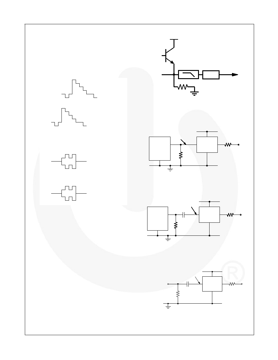
Functional Description
The FMS6363 Low-Cost Video Filter (LCVF) provides
6dB gain from input to output. In addition, the input is
slightly offset to optimize the output driver performance.
The offset is held to the minimum required value to
decrease the standing DC current into the load. Typical
voltage levels are shown in Figure 8.
There will be a 280mV offset from the DC input level to
the DC output level.
Vout = 2 * Vin + 280mV
0.02V
0.32V
1.02V
VIN
0.15V
0.5V
0.85V
VIN
0.28V
0.88V
2.28V
Driven by:
DC-Coupled DAC Outputs o r
AC-Coupled and Clamped
Y, R, G, B, CV
VOUT
0.58V
1.28V
1.98V
Driven by:
DC-Coupled DAC Outputs
AC-Coupled and Biased
U, V, Pb, Pr, C
VOUT
Figure 8. Typical Voltage Levels
The FMS6363 provides an internal diode clamp to
support AC coupled input signals. If the input signal
does not go below ground, the input clamp does not
operate. This allows DAC outputs to directly drive the
FMS6363 without an AC coupling capacitor. The worst-
case sync tip compression due to the clamp does not
exceed 7mV. The input level set by the clamp,
combined with the internal DC offset, keeps the output
within its acceptable range. When the input is AC-
coupled, the diode clamp sets the sync tip (or lowest
voltage) just below ground.
For symmetric signals like C, U, V, Cb, Cr, Pb and Pr;
the average DC bias is fairly constant and the inputs
can be AC-coupled with the addition of a pull-up resistor
to set the DC input voltage. DAC outputs can also drive
these same signals without the AC coupling capacitor.
A conceptual illustration of the input clamp circuit is
shown in Figure 9.
YOUT
800k
Driver
YIN
0.65V
Figure 9. Input Clamp Circuit
I/O Configurations
For DC-coupled DAC drive with DC-coupled outputs,
use the configuration in Figure 10.
DVD or
STB
SoC
DAC
Output
75
Ω
LCVF
Clamp
Inactive
0V- 1.4V
Figure 10. DC-coupled Inputs and Outputs
Alternatively, if the DAC’s average DC output level
causes the signal to exceed the range of 0V to 1.4V, it
can be AC-coupled, as shown in Figure 11.
DVD or
STB
SoC
DAC
Output
75
Ω
LCVF
Clamp
Active
0.1
0V- 1.4V
Figure 11. AC-coupled Inputs, DC-coupled Outputs
When the FMS6363 is driven by an unknown external
source or a SCART with its own clamping circuitry the
inputs should be AC-coupled, shown in Figure 12.
75
Ω
LCVF
Clamp
Active
75
Ω
0.1
External Video
source must
be AC-coupled.
0V- 1.4V
Figure 12. SCART with DC-coupled Outputs
相关PDF资料 |
PDF描述 |
|---|---|
| FMS6364AMTC14X | IC DVR VID FILTER SD/HD 14TSSOP |
| FMS6403MTC20 | IC DRIVER VID TRPL FLTR 20TSSOP |
| FMS6404CSX | IC DVR VID 5TH BUTTERWORTH 8SOIC |
| FMS6406CS | IC FILTER S-VIDEO DUAL 8SOIC |
| FMS6410BCS | IC FILTER VIDEO DUAL 8SOIC |
相关代理商/技术参数 |
参数描述 |
|---|---|
| FMS6363CS_NL | 制造商:Fairchild Semiconductor Corporation 功能描述: |
| FMS6363CSX | 功能描述:视频 IC MSFG LoCst3Chnl6th HI DefVidFiltrDrivr RoHS:否 制造商:Fairchild Semiconductor 工作电源电压:5 V 电源电流:80 mA 最大工作温度:+ 85 C 封装 / 箱体:TSSOP-28 封装:Reel |
| FMS6363CSX_NL | 功能描述:视频 IC Video Filter Driver 3-Ch High Def RoHS:否 制造商:Fairchild Semiconductor 工作电源电压:5 V 电源电流:80 mA 最大工作温度:+ 85 C 封装 / 箱体:TSSOP-28 封装:Reel |
| FMS6364A | 制造商:FAIRCHILD 制造商全称:Fairchild Semiconductor 功能描述:Low-Cost Four-Channel Standard Definition (SD) & High (HD) Definition Video Filter Driver |
| FMS6364AMTC14X | 功能描述:显示驱动器和控制器 LW COST 4CH SD/HD Video Filter Driver RoHS:否 制造商:Panasonic Electronic Components 工作电源电压:2.7 V to 5.5 V 最大工作温度: 安装风格:SMD/SMT 封装 / 箱体:QFN-44 封装:Reel |
发布紧急采购,3分钟左右您将得到回复。