- 您现在的位置:买卖IC网 > PDF目录16985 > FPF1016 (Fairchild Semiconductor)IC LOAD SWITCH 1V ADVANCED 6UMLP PDF资料下载
参数资料
| 型号: | FPF1016 |
| 厂商: | Fairchild Semiconductor |
| 文件页数: | 8/11页 |
| 文件大小: | 0K |
| 描述: | IC LOAD SWITCH 1V ADVANCED 6UMLP |
| 产品变化通告: | Pkg Change 13/Jul/2009 |
| 标准包装: | 3,000 |
| 系列: | IntelliMax™ |
| 类型: | 高端开关 |
| 输出数: | 1 |
| Rds(开): | 45 毫欧 |
| 内部开关: | 是 |
| 电流限制: | 1.5A |
| 输入电压: | 0.8 V ~ 1.8 V |
| 工作温度: | -40°C ~ 85°C |
| 安装类型: | 表面贴装 |
| 封装/外壳: | 6-UMLP |
| 供应商设备封装: | 6-UMLP(2x2) |
| 包装: | 带卷 (TR) |
�� �
�
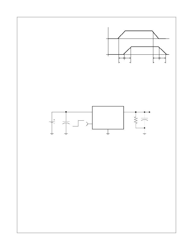
�Description� of� Operation�
�Timing� Diagram�
�The� FPF1015/6/7/8� are� low� R� DS(ON)� N-Channel� load� switches�
�with� controlled� turn-on.� The� core� of� each� device� is� a� 34m� ?�
�(V� IN� =� 1V,� V� ON� =� 3V)� N-Channel� MOSFET� and� is� customized� for�
�a� low� input� operating� range� of� 0.8� to� 1.8V.� The� ON� pin� controls�
�V� ON�
�10%�
�90%�
�the� state� of� the� switch.�
�The� FPF1016� and� FPF1018� contain� a� 60� ?� (typ)� on-chip� resistor�
�90%�
�90%�
�which� is� connected� internally� from� V� OUT� to� GND� for� quick� output�
�discharge� when� the� switch� is� turned� off.�
�On/Off� Control�
�The� ON� pin� is� active� high� and� it� controls� the� state� of� the� switch.�
�V� OUT�
�10%�
�td� ON� t� R�
�t� ON�
�where:�
�td� OFF� t� F�
�t� OFF�
�10%�
�Applying� a� continuous� high� signal� will� hold� the� switch� in� the� ON�
�state.� In� order� to� minimize� the� switch� on� resistance,� the� ON� pin�
�voltage� should� exceed� the� input� voltage� by� 2V.� This� device� is�
�compatible� with� a� GPIO� (General� Purpose� Input/Output)� port,�
�where� the� logic� voltage� level� can� be� configured� to� 4V� ≥� V� ON� ≥�
�V� IN� +2V� and� power� consumed� is� less� than� 1μA� in� steady� state.�
�td� ON�
�t� R�
�t� ON�
�td� OFF�
�t� F�
�t� OFF�
�=�
�=�
�=�
�=�
�=�
�=�
�Delay� On� Time�
�V� OUT� Rise� Time�
�Turn� On� Time�
�Delay� Off� Time�
�V� OUT� Fall� Time�
�Turn� Off� Time�
�Application� Information�
�Typical� Application�
�V� IN�
�V� OUT�
�V� IN� =� 0.8-1.8V�
�C� IN�
�OFF� ON�
�ON�
�FPF1015/6/7/8�
�R� L�
�C� L�
�GND�
�Input� Capacitor�
�To� limit� the� voltage� drop� on� the� input� supply� caused� by� transient�
�in-rush� currents� when� the� switch� turns-on,� a� capacitor� must� be�
�placed� between� V� IN� and� GND.� For� minimized� voltage� drop,�
�especially� when� the� operating� voltage� approaches� 1V� and� a� fast�
�slew� rate� part� (FPF1015� and� FPF1016)� is� selected,� a� 10μF�
�ceramic� capacitor� should� be� placed� close� to� the� V� IN� pins.� Higher�
�values� of� C� IN� can� be� used� to� further� reduce� the� voltage� drop�
�during� higher� current� modes� of� operation.�
�Output� Capacitor�
�A� 0.1μF� capacitor,� C� L� ,� should� be� placed� between� V� OUT� and�
�GND.� This� capacitor� will� prevent� parasitic� board� inductance�
�from� forcing� V� OUT� below� GND� when� the� switch� turns-off.� If� the�
�application� has� a� capacitive� load,� the� FPF1016� and� FPF1018�
�can� be� used� to� discharged� that� load� through� an� on-chip� output�
�discharge� path.�
�Board� Layout�
�For� best� performance,� all� traces� should� be� as� short� as� possible.�
�To� be� most� effective,� the� input� and� output� capacitors� should� be�
�placed� close� to� the� device� to� minimize� the� effects� that� parasitic�
�trace� inductances� may� have� on� normal� and� short-circuit�
�operation.� Using� wide� traces� or� large� copper� planes� for� all� pins�
�(V� IN� ,� V� OUT� ,� ON� and� GND)� will� help� minimize� the� parasitic�
�electrical� effects� along� with� minimizing� the� case� to� ambient�
�thermal� impedance.�
�FPF1015/6/7/8� Rev.� D�
�8�
�www.fairchildsemi.com�
�相关PDF资料 |
PDF描述 |
|---|---|
| FPF1015 | IC LOAD SWITCH 1V ADVANCED 6UMLP |
| HFI-201209-R15J | INDUCTOR 2.0X1.2X0.9MM 150NH |
| OPAMPEVM-SOT23SHDN | UNIV EVAL MOD FOR SOT23 PKG |
| VE-25H-EY | CONVERTER MOD DC/DC 52V 50W |
| MLG1005S0N8C | INDUCTOR MULTILAYER 0.8NH 0402 |
相关代理商/技术参数 |
参数描述 |
|---|---|
| FPF1017 | 功能描述:电源开关 IC - 配电 Intellimax Advanced Load Manag Products RoHS:否 制造商:Exar 输出端数量:1 开启电阻(最大值):85 mOhms 开启时间(最大值):400 us 关闭时间(最大值):20 us 工作电源电压:3.2 V to 6.5 V 电源电流(最大值): 最大工作温度:+ 85 C 安装风格:SMD/SMT 封装 / 箱体:SOT-23-5 |
| FPF1018 | 功能描述:电源开关 IC - 配电 Intellimax Advanced Load Manag Products RoHS:否 制造商:Exar 输出端数量:1 开启电阻(最大值):85 mOhms 开启时间(最大值):400 us 关闭时间(最大值):20 us 工作电源电压:3.2 V to 6.5 V 电源电流(最大值): 最大工作温度:+ 85 C 安装风格:SMD/SMT 封装 / 箱体:SOT-23-5 |
| FPF1026_AAB3026D WAF | 制造商:Fairchild Semiconductor Corporation 功能描述: |
| FPF1026_AAB3086D WAF | 制造商:Fairchild Semiconductor Corporation 功能描述: |
| FPF1038 | 制造商:FAIRCHILD 制造商全称:Fairchild Semiconductor 功能描述:Low On-Resistance, Slew-Rate-Controlled Load Switch |
发布紧急采购,3分钟左右您将得到回复。