参数资料
| 型号: | FS7145-02G-XTP |
| 厂商: | ON Semiconductor |
| 文件页数: | 13/17页 |
| 文件大小: | 0K |
| 描述: | IC CLOCK GEN PLL PROG 16SSOP |
| 标准包装: | 1,500 |
| 类型: | 时钟/频率合成器 |
| PLL: | 是 |
| 输入: | 晶体 |
| 输出: | CMOS,PECL |
| 电路数: | 1 |
| 比率 - 输入:输出: | 2:1 |
| 差分 - 输入:输出: | 无/是 |
| 频率 - 最大: | 300MHz |
| 除法器/乘法器: | 是/无 |
| 电源电压: | 3 V ~ 3.6 V |
| 工作温度: | 0°C ~ 70°C |
| 安装类型: | 表面贴装 |
| 封装/外壳: | 16-SSOP(0.209",5.30mm 宽) |
| 供应商设备封装: | 16-SSOP |
| 包装: | 带卷 (TR) |
FS7140, FS7145
http://onsemi.com
5
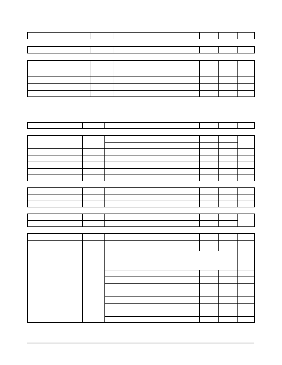
Parameter
Units
Max
Typ
Min
Conditions/Description
Symbol
CLOCK OUTPUTS, CMOS MODE (CLKN, CLKP)
Lowlevel output sink current
IOL
VO = 0.4 V
35
mA
CLOCK OUTPUTS, PECL MODE (CLKN, CLKP)
IPRG bias voltage
VIPRG
VIPRG will be clamped to this level
when a resistor is connected from
VDD to IPRG
VDD/3
V
IPRG bias current
IIPRG
IIPRG (VVDD VIPRG) / RSET
3.5
mA
Sink current to IPRG current ratio
13
Tristate output current
IZ
10
mA
1. Unless otherwise stated, VDD = 3.3 V ± 10%, no load on any output, and ambient temperature range TA = 0°C to 70°C. Parameters denoted
with an asterisk (*) represent nominal characterization data and are not production tested to any specific limits. MIN and MAX characteriza-
tion data are ± 3s from typical. Negative currents indicate flows out of the device.
Table 5. AC TIMING SPECIFICATIONS (Note 2)
Parameter
Symbol
Conditions/Description
Min
Typ
Max
Units
OVERALL
Output frequency*
fo(max)
CMOS outputs
0
150
MHz
PECL outputs
0
300
VCO frequency*
fVCO
40
400
MHz
CMOS mode rise time*
tr
CL = 7 pF
1
ns
CMOS mode fall time*
tf
CL = 7 pF
1
ns
PECL mode rise time*
tr
CL = 7 pF; RL = 65 ohm
1
ns
PECL mode fall time*
tf
CL = 7 pF; RL = 65 ohm
1
ns
REFERENCE FREQUENCY INPUT (REF)
Input frequency
FREF
80
MHz
Reference high time
tREHF
3
ns
Reference low time
tREFL
3
ns
SYNC CONTROL INPUT (SYNC)
Sync high time
tSYNCH
For orderly CLK stop/start
3
TCLK
Sync low time
tSYNCL
For orderly CLK stop/start
3
CLOCK OUTPUT (CLKN, CLKP)
Duty cycle (CMOS mode)*
Measured at 1.4 V
50
%
Duty cycle (PECL mode)*
Measured at zero crossings of
(VCLKP VCLKN)
50
%
Jitter, long term (sy(t))*
tj(LT)
For valid programming solutions. Long-term (or cumulative) jitter specified is
RMS position error of any edge compared with an ideal clock generated from
the same reference frequency. It is measured with a time interval analyzer us-
ing a 500 microsecond window, using statistics gathered over 1000 samples.
ps
FREF/NREF > 1000 kHz
25
ps
FREF/NREF ^ 500 kHz
50
ps
FREF/NREF ^ 250 kHz
100
ps
FREF/NREF ^ 125 kHz
190
ps
FREF/NREF ^ 62.5 kHz
240
ps
FREF/NREF ^ 31.5 kHz
300
ps
Jitter, period (peakpeak)*
tj(DP)
40 MHz < VCO frequency < 100 MHz
75
ps
VCO frequency > 100 MHz
50
ps
2. Unless otherwise stated, VDD = 3.3 V ± 10%, no load on any output, and ambient temperature range TA = 0°C to 70°C. Parameters denoted
with an asterisk (*) represent nominal characterization data and are not production tested to any specific limits. MIN and MAX characterization
data are ± 3s from typical.
相关PDF资料 |
PDF描述 |
|---|---|
| VE-B1Y-MY-F2 | CONVERTER MOD DC/DC 3.3V 33W |
| GTC02R-28-15S | CONN RCPT 35POS BOX MNT W/SCKT |
| VI-JV0-MZ-F1 | CONVERTER MOD DC/DC 5V 25W |
| VI-25H-MW-F1 | CONVERTER MOD DC/DC 52V 100W |
| MS27472E24F2SB | CONN RCPT 100POS WALL MT W/SCKT |
相关代理商/技术参数 |
参数描述 |
|---|---|
| FS714X | 制造商:ONSEMI 制造商全称:ON Semiconductor 功能描述:Programmable Phase-Locked Loop Clock Generator |
| FS7-4 | 制造商:未知厂家 制造商全称:未知厂家 功能描述:Flow Switches - Liquid |
| FS7-4D | 制造商:未知厂家 制造商全称:未知厂家 功能描述:Flow Switches - Liquid |
| FS7-4DF | 制造商:未知厂家 制造商全称:未知厂家 功能描述:Flow Switches - Liquid |
| FS7-4DS | 制造商:未知厂家 制造商全称:未知厂家 功能描述:Flow Switches - Liquid |
发布紧急采购,3分钟左右您将得到回复。