- 您现在的位置:买卖IC网 > PDF目录1922 > FSSD06BQX (Fairchild Semiconductor)IC MUX SD/SDIO/MMC 2PORT 24-MLP PDF资料下载
参数资料
| 型号: | FSSD06BQX |
| 厂商: | Fairchild Semiconductor |
| 文件页数: | 8/14页 |
| 文件大小: | 0K |
| 描述: | IC MUX SD/SDIO/MMC 2PORT 24-MLP |
| 标准包装: | 1 |
| 类型: | 多路复用器 |
| 应用: | 手机,数码相机,媒体播放器 |
| 安装类型: | 表面贴装 |
| 封装/外壳: | 24-MLP |
| 供应商设备封装: | 24-MLP(5x5) |
| 包装: | 标准包装 |
| 产品目录页面: | 1219 (CN2011-ZH PDF) |
| 其它名称: | FSSD06BQXDKR |
2007 Fairchild Semiconductor Corporation
www.fairchildsemi.com
FSSD06 Rev. 1.0.5
3
FSSD06
—
SD/SDIO
and
MMC
Two-Port
Multiplexer
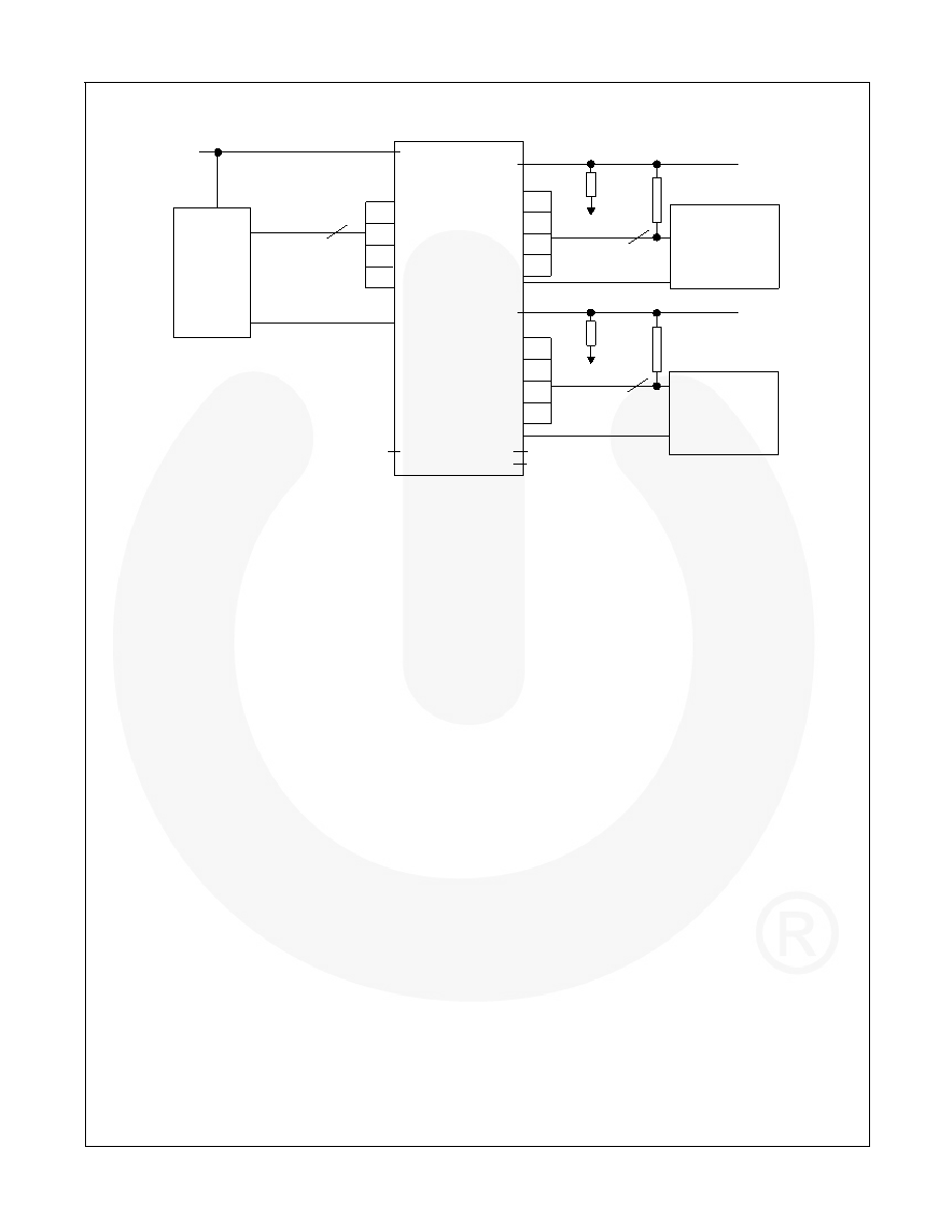
Typical Application Diagram
CMD, DAT[3:0]
5
1.65 – 3.60V
WiFi,
Bluetooth,
MMC or SD
Module
Processor
VDDH
GND
/OE
S
1CMD, 1DAT[3:0]
FSSD06
Secure Data /
Multimedia Card
2:1 Peripheral
Expander
CLK
1CLK
5
2CMD, 2DAT[3:0]
WiFi,
Bluetooth,
MMC or SD
Module
,,
2CLK
5
V
DD H to 3.6V
VDDC1
V
DD H to 3.6V
VDDC2
GND
RT
GND
RT
Note
: External resistors (R T) are
recommended if card supplies are
allowed to float in the application.
The resistors should be >500K to
minimize power consumption.
Figure 4.
Typical Application Diagram
Functional Description
The FSSD06 enables sharing the ASIC/baseband
processor SDIO port(s) to two peripheral cards,
providing
bi-directional
support
for
dual-voltage
SD/SDIO or MMC cards available in the marketplace.
Each SDIO port of the FSSD06 has its own supply rail,
allowing peripheral cards with different supplies to be
interfaced to the host. The peripheral card supplies must
be equal or greater than the host to minimize power
consumption. The independent VDDH, VDDC1, and VDDC2
are defined by the supplies connected from the
application Power Management ICs (PMICs) to the
FSSD06. The clock path is a uni-directional buffered
path rather than a bi-directional switch port.
CMD, DAT Bus Pull-ups
The 1CMD, 2CMD, 1DAT[3:0], and 2DAT[3:0] ports do
not have, internally, the system pull-up resistors as
defined in the MMC or SD card system bus
specifications. The system bus pull-up must be added
external to the FSSD06. The value, within the specific
specification limits, is a function of the individual
application and type of card or peripheral connected. For
SD card applications, the RCMD and RDAT pull-ups should
be between 10k and 100k. For MMC applications,
the RCMD pull-ups should be between 4.7k and 100k
and the RDAT pull-ups between 50k and 100k. The
card-side 1CMD, 2CMD, 1DAT[3:0], and 2DAT[3:0]
outputs have a circuit that facilitates incident wave
switching, so the external pull-up resistors ensure
retention of the output high level.
The /OE pin can be used to place the 1CMD, 2CMD,
1DAT[3:0] and 2DAT[3:0] into high-impedance mode
when the system enters IDLE state (see IDLE State
CMD/DAT Bus “Parking”
).
CLK Bus
The 1CLK and 2CLK outputs are bi-state buffer
architectures, rather than a switch I/O, to ensure 52MHz
incident
wave
switching.
When
there
is
no
communication on the bus (IDLE), the FSSD06 can be
disabled with the /OE pin. When this pin is pulled HIGH,
the nCLK outputs are also pulled HIGH. Along with
nCMD, nDAT[3:0] goes high-impedance to ensure that
the CLK path between the FSSD06 and the peripheral
does not float.
IDLE State CMD/DAT Bus “Parking”
The SD and MMC card specifications were written for a
direct point-to-point communication between host
controller and card. The introduction of the FSSD06 in
that path, as an expander, requires that the functional
operation and system latency not be impacted by the
FSSD06 switch characteristics. Since there are various
card formats, protocols, and configurable controllers, a
/OE pin is available to facilitate a fast IDLE transition for
the nCMD/nDAT[3:0] outputs. Some controllers, rather
than simply placing CMD/DAT into high-impedance
mode, may pull their outputs HIGH for a clock cycle prior
to going into high-impedance mode (referred to as
“parking” the output). Some legacy controllers pull their
outputs HIGH versus high impedance.
If the /OE pin is left LOW and the controller places the
CMD/DAT[3:0] outputs into high impedance, the
nCMD/nDAT[3:0] output rise time is a function of the RC
time
constant
through
the
switch
path.
It
is
recommended that the host controller pull CMD and
DAT[3:0] HIGH for one cycle before pulling /OE HIGH.
This facilitates parking all nCMD/nDAT[3:0] outputs
HIGH before putting the switch I/Os in high impedance.
相关PDF资料 |
PDF描述 |
|---|---|
| FSSD07BQX | IC MUX 2:1 SD/SDIO/MMC 24-MLP |
| FSTU32160MTDX | IC MUX/DEMUX 1X2 56TSSOP |
| FSUSB104UMX | IC USB SWITCH DUAL DPDT 10UMLP |
| FSUSB11L10X | IC USB SWIT DUAL 1X1 10MICROPAK |
| FSUSB20L10X | IC USB SWIT DUAL 2X1 10MICROPAK |
相关代理商/技术参数 |
参数描述 |
|---|---|
| FSSD06BQX_12 | 制造商:FAIRCHILD 制造商全称:Fairchild Semiconductor 功能描述:SD/SDIO and MMC Two-Port Multiplexer |
| FSSD06UMX | 功能描述:开关 IC - 各种 Multiplexer 24-Pin UMLP EP RoHS:否 制造商:Fairchild Semiconductor 开启电阻(最大值): 电源电压-最大:4.4 V 电源电压-最小:2.5 V 最大工作温度:+ 85 C 最小工作温度:- 40 C 封装 / 箱体:WLCSP-9 封装:Reel |
| FSSD06UMX_12 | 制造商:FAIRCHILD 制造商全称:Fairchild Semiconductor 功能描述:SD/SDIO and MMC Two-Port Multiplexer |
| FSSD07 | 制造商:FAIRCHILD 制造商全称:Fairchild Semiconductor 功能描述:1-Bit / 4-Bit SD/SDIO and MMC Dual-Host Multiplexer |
| FSSD07_12 | 制造商:FAIRCHILD 制造商全称:Fairchild Semiconductor 功能描述:1-Bit / 4-Bit SD/SDIO and MMC Dual-Host Multiplexer |
发布紧急采购,3分钟左右您将得到回复。