- 您现在的位置:买卖IC网 > PDF目录370249 > FSTUD32450GX BUS SWITCH|CMOS|BGA|114PIN|PLASTIC PDF资料下载
参数资料
| 型号: | FSTUD32450GX |
| 英文描述: | BUS SWITCH|CMOS|BGA|114PIN|PLASTIC |
| 中文描述: | 总线开关|的CMOS | BGA封装| 114PIN |塑料 |
| 文件页数: | 9/13页 |
| 文件大小: | 474K |
| 代理商: | FSTUD32450GX |
9
www.fairchildsemi.com
F
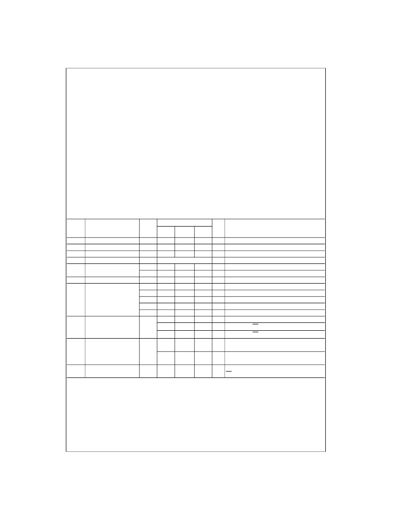
Absolute Maximum Ratings
(Note 2)
Recommended Operating
Conditions
(Note 5)
Note 2:
The
“
Absolute Maximum Ratings
”
are those values beyond which
the safety of the device cannot be guaranteed. The device should not be
operated at these limits. The parametric values defined in the Electrical
Characteristics tables are not guaranteed at the absolute maximum rating.
The
“
Recommended Operating Conditions
”
table will define the conditions
for actual device operation.
Note 3:
V
S
is the voltage observed/applied at either the A or B Ports across
the switch.
Note 4:
The input and output negative voltage ratings may be exceeded if
the input and output diode current ratings are observed.
Note 5:
Unused control inputs must be held HIGH or LOW. They may not
float.
DC Electrical Characteristics
Note 6:
Typical values are at V
CC
=
5.0V and T
A
=
+
25
°
C
Note 7:
Measured by the voltage drop between A and B pins at the indicated current through the switch. On Resistance is determined by the lower of the
voltages on the two (A or B) pins.
Supply Voltage (V
CC
)
DC Switch Voltage (V
S
) (Note 3)
DC Input Control Pin Voltage
(V
IN
) (Note 4)
DC Input Diode Current (l
IK
) V
IN
<
0V
DC Output (I
OUT
) Current
DC V
CC
/GND Current (I
CC
/I
GND
)
Storage Temperature Range (T
STG
)
0.5V to
+
7.0V
2.0V to
+
7.0V
0.5V to
+
7.0V
50 mA
128 mA
+
/
100 mA
65
°
C to
+
150
°
C
Power Supply Operating (V
CC)
Input Voltage (V
IN
)
Output Voltage (V
OUT
)
Free Air Operating Temperature (T
A
)
4.0V to 5.5V
0V to 5.5V
0V to 5.5V
-40
°
C to
+
85
°
C
Symbol
Parameter
V
CC
(V)
T
A
=
40
°
C to
+
85
°
C
Min
Typ
(Note 6)
Units
Conditions
Max
V
IK
V
IH
V
IL
V
OH
I
I
Clamp Diode Voltage
HIGH Level Input Voltage
4.5
1.2
V
V
I
IN
=
18 mA
IF S
2
=
HIGH
IF S
2
=
HIGH
S
2
=
S
5
=
V
CC
0
≤
V
IN
≤
5.5V
V
IN
=
5.5V
0
≤
A, B
≤
V
CC
V
IN
=
0V, I
IN
=
64 mA, S
2
=
S
5
=
0V or V
CC
V
IN
=
0V, I
IN
=
30 mA, S
2
=
S
5
=
0V or V
CC
V
IN
=
2.4V, I
IN
=
15 mA, S
2
=
S
5
=
0V
V
IN
=
2.4V, I
IN
=
15 mA, S
2
=
S
5
=
0V
V
IN
=
2.4V, I
IN
=
15 mA, S
2
=
S
5
=
V
CC
S
2
=
S
5
=
GND, V
IN
=
V
CC
or GND, I
OUT
=
0
4.0-5.5
2.0
4.5V
≤
V
CC
≤
5.5V
4.5V
≤
V
CC
≤
5.5V
LOW Level Input Voltage
HIGH Level Output Voltage
Input Leakage Current
4.0-5.5
4.5-5.5
5.5
0.8
V
V
μ
A
μ
A
μ
A
μ
A
See Figure 4
±
1.0
10
±
1.0
7
0
I
OZ
R
ON
OFF-STATE Leakage Current
Switch On Resistance
5.5
4.5
4
(Note 7)
4.5
4.5
4.0
4
8
11
7
12
20
4.5
35
50
3
I
CC
Quiescent Supply Current
5.5
10
μ
A
S
2
=
S
5
=
V
CC
, OE
x
=
V
CC
, V
IN
=
V
CC
or GND, I
OUT
=
0
1.5
mA
S
2
=
S
5
=
V
CC
, OE
x
=
GND, V
IN
=
V
CC
or GND, I
OUT
=
0
One Input at 3.4V
Other Inputs at V
CC
or GND, S
2
=
0V
One Input at 3.4V
Other Inputs at V
CC
or GND, S
2
=
V
CC
0.0 mA
≥
I
IN
≥
50 mA
OE
x
=
5.5V
I
CC
Increase in I
CC
per Input
5.5
2.5
mA
4.0
mA
V
IKU
Voltage Undershoot
5.5
2.0
V
相关PDF资料 |
PDF描述 |
|---|---|
| FSU05B60 | FOR POWER FACTOR IMPROVEMENT HIGH FREQUENCY RECTIFICATION |
| FSU10B60 | FOR POWER FACTOR IMPROVEMENT HIGH FREQUENCY RECTIFICATION |
| FSU10A30 | For Power Factor Improvement High Frequency Rectification |
| FSYC9260D1 | TRANSISTOR | MOSFET | P-CHANNEL | 200V V(BR)DSS | 28A I(D) | SMT |
| FSYC9260D3 | TRANSISTOR | MOSFET | P-CHANNEL | 200V V(BR)DSS | 28A I(D) | SMT |
相关代理商/技术参数 |
参数描述 |
|---|---|
| FSTUD32450GX_NL | 制造商:Rochester Electronics LLC 功能描述: 制造商:Fairchild Semiconductor Corporation 功能描述: |
| FSTVK-01 | 制造商:QUEST TECHNOLOGY 功能描述:Cord Cover Kit for flat screen TVs, 48in x 3in x 1in, white |
| FSTVK-02 | 制造商:QUEST TECHNOLOGY 功能描述:Cord cover Kit for flat screen TVs. 48in x 3in x 1in, beige |
| FSTY | 功能描述:手工工具 Fiber Optic Clean Up Book, Sticky Clear RoHS:否 制造商:Molex 产品:Extraction Tools 类型: 描述/功能:Extraction tool |
| FSTYC9055D | 制造商:INTERSIL 制造商全称:Intersil Corporation 功能描述:Radiation Hardened, SEGR Resistant P-Channel Power MOSFETs |
发布紧急采购,3分钟左右您将得到回复。