- 您现在的位置:买卖IC网 > PDF目录67595 > G2995P1UF (Global Mixed-mode Technology Inc.) DDR Termination Regulator PDF资料下载
参数资料
| 型号: | G2995P1UF |
| 厂商: | Global Mixed-mode Technology Inc. |
| 英文描述: | DDR Termination Regulator |
| 中文描述: | DDR终端稳压器 |
| 文件页数: | 2/12页 |
| 文件大小: | 272K |
| 代理商: | G2995P1UF |
Ver: 1.7
May 10, 2005
TEL: 886-3-5788833
http://www.gmt.com.tw
10
G2995
Global Mixed-mode Technology Inc.
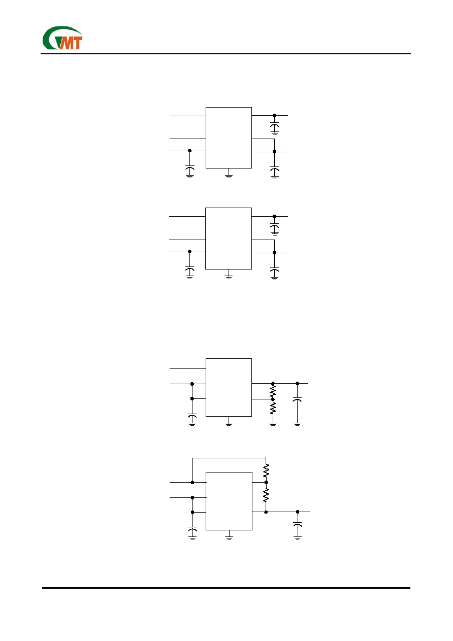
In Figure 5 & 6, they are the application configurations
of DDR-II SDRAM bus terminations. Figure 5 is the
typical application scheme of DDR-II SDRAM. With the
separate VDDQ pin and an internal resistor divider, it
is possible to use the G2995 in applications utilizing
DDR-II memory. Figure 6 is used to increase the driv-
ing capability. The risk is the same as figure 4.
Figure 7 & 8 are used to scale the VTT to the wanted
value when the standard voltages of SSTL-2 do not
meet the requirements. Using R1 & R2, Figure 7 can
shift VTT up to VDDQ/2 * (1+R1/R2) and figure 8 can
shift VTT down to VDDQ/2 * (1-R1/R2).
+
V
DDQ
AV
IN
V
SENSE
PV
IN
V
TT
GND
V
TT
V
DD
C
IN
Figure 7. Increasing VTT by Level Shifting
C
OUT
V
DDQ
R1
R2
+
V
DDQ
AV
IN
V
SENSE
PV
IN
V
TT
GND
V
TT
V
DD
C
IN
Figure 8. Decreasing VTT by Level Shifting
C
OUT
V
DDQ
R1
R2
+
V
DDQ
AV
IN
V
SENSE
PV
IN
V
TT
GND
V
TT
V
DD
C
IN
Figure 7. Increasing VTT by Level Shifting
C
OUT
V
DDQ
R1
R2
+
V
DDQ
AV
IN
V
SENSE
PV
IN
V
TT
GND
V
TT
V
DD
C
IN
Figure 7. Increasing VTT by Level Shifting
C
OUT
V
DDQ
R1
R2
+
V
DDQ
AV
IN
V
SENSE
PV
IN
V
TT
GND
V
TT
V
DD
C
IN
Figure 8. Decreasing VTT by Level Shifting
C
OUT
V
DDQ
R1
R2
+
V
DDQ
AV
IN
V
SENSE
PV
IN
V
TT
GND
V
TT
V
DD
C
IN
Figure 8. Decreasing VTT by Level Shifting
C
OUT
V
DDQ
R1
R2
+
V
REF
V
DDQ
AV
IN
V
SENSE
PV
IN
V
TT
GND
V
TT=0.9V
V
REF=0.9V
V
DDQ=1.8V
AV
IN=1.8V or 5.5V
C
IN
Figure 5. Recommended DDR-II Termination
C
OUT
C
REF
PV
IN=1.8V
+
V
REF
V
DDQ
AV
IN
V
SENSE
PV
IN
V
TT
GND
V
TT=0.9V
V
REF=0.9V
V
DDQ=1.8V
AV
IN=3.3V or 5.5V
C
IN
Figure 6. DDR-II Termination with higher voltage rails
C
OUT
C
REF
PV
IN=3.3V
+
V
REF
V
DDQ
AV
IN
V
SENSE
PV
IN
V
TT
GND
V
TT=0.9V
V
REF=0.9V
V
DDQ=1.8V
AV
IN=1.8V or 5.5V
C
IN
Figure 5. Recommended DDR-II Termination
C
OUT
C
REF
PV
IN=1.8V
+
V
REF
V
DDQ
AV
IN
V
SENSE
PV
IN
V
TT
GND
V
TT=0.9V
V
REF=0.9V
V
DDQ=1.8V
AV
IN=3.3V or 5.5V
C
IN
Figure 6. DDR-II Termination with higher voltage rails
C
OUT
C
REF
PV
IN=3.3V
相关PDF资料 |
PDF描述 |
|---|---|
| G2996F1UF | DDR I/II Termination Regulator |
| G2996F1U | DDR I/II Termination Regulator |
| G2996P1UF | DDR I/II Termination Regulator |
| G2996P1U | DDR I/II Termination Regulator |
| G5105TBU | Low-Noise Step-up DC-DC Converter |
相关代理商/技术参数 |
参数描述 |
|---|---|
| G2996 | 制造商:未知厂家 制造商全称:未知厂家 功能描述:DDR Termination Regulator with STR function.|Terminator Series |
| G2996F1U | 制造商:GMT 制造商全称:Global Mixed-mode Technology Inc 功能描述:DDR I/II Termination Regulator |
| G2996F1UF | 制造商:GMT 制造商全称:Global Mixed-mode Technology Inc 功能描述:DDR I/II Termination Regulator |
| G2996P1U | 制造商:GMT 制造商全称:Global Mixed-mode Technology Inc 功能描述:DDR I/II Termination Regulator |
| G2996P1UF | 制造商:GMT 制造商全称:Global Mixed-mode Technology Inc 功能描述:DDR I/II Termination Regulator |
发布紧急采购,3分钟左右您将得到回复。