- 您现在的位置:买卖IC网 > PDF目录1922 > GAL18V10B-20LP (Lattice Semiconductor Corporation)IC GAL 10OUT MACROCELL 7.5NS 20 PDF资料下载
参数资料
| 型号: | GAL18V10B-20LP |
| 厂商: | Lattice Semiconductor Corporation |
| 文件页数: | 8/15页 |
| 文件大小: | 0K |
| 描述: | IC GAL 10OUT MACROCELL 7.5NS 20 |
| 产品变化通告: | Product Discontinuation 07/Sept/2010 |
| 标准包装: | 1 |
| 可编程类型: | EE PLD |
| 宏单元数: | 10 |
| 输入电压: | 4.75 V ~ 5.25 V |
| 速度: | 20ns |
| 安装类型: | 通孔 |
| 封装/外壳: | 20-DIP(0.300",7.62mm) |
| 供应商设备封装: | 20-PDIP |
| 包装: | 管件 |
| 其它名称: | Q6330552 |
GAL18V10
High Performance E2CMOS PLD
Generic Array Logic
1
2
20
I/CLK
I
Vcc
I/O/Q
I
GND
I/O/Q I/O/Q
I/O/Q
4
6
8
9
11
13
14
16
18
1
10
11
20
I/CLK
I
I/O/Q
GND
Vcc
I/O/Q
5
15
GAL18V10
Top View
GAL
18V10
DIP
PLCC
I/O/Q
I/CLK
RESET
PRESET
8
10
8
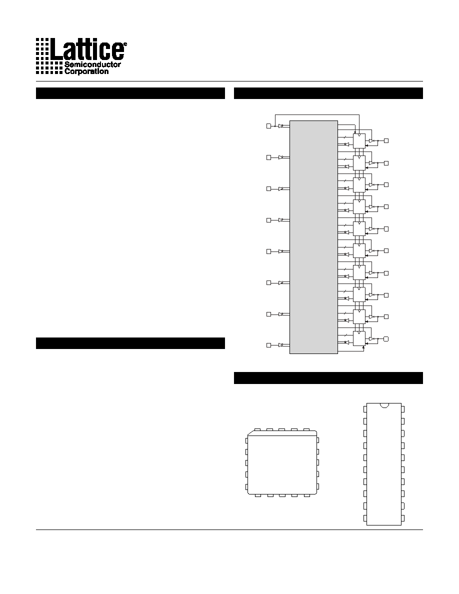
OLMC
I
PROGRAMMABLE
AND-ARRAY
(96X36)
Copyright 2003 Lattice Semiconductor Corp. All brand or product names are trademarks or registered trademarks of their respective holders. The specifications and information herein are subject
to change without notice.
LATTICE SEMICONDUCTOR CORP., 5555 Northeast Moore Ct., Hillsboro, Oregon 97124, U.S.A.
November 2003
Tel. (503) 268-8000; 1-800-LATTICE; FAX (503) 268-8556; http://www.latticesemi.com
18v10_04
Features
HIGH PERFORMANCE E2CMOS TECHNOLOGY
— 7.5 ns Maximum Propagation Delay
— Fmax = 111 MHz
— 5.5 ns Maximum from Clock Input to Data Output
— TTL Compatible 16 mA Outputs
— UltraMOS Advanced CMOS Technology
LOW POWER CMOS
— 75 mA Typical Icc
ACTIVE PULL-UPS ON ALL PINS
E2 CELL TECHNOLOGY
— Reconfigurable Logic
— Reprogrammable Cells
— 100% Tested/100% Yields
— High Speed Electrical Erasure (<100ms)
— 20 Year Data Retention
TEN OUTPUT LOGIC MACROCELLS
— Uses Standard 22V10 Macrocell Architecture
— Maximum Flexibility for Complex Logic Designs
PRELOAD AND POWER-ON RESET OF REGISTERS
— 100% Functional Testability
APPLICATIONS INCLUDE:
— DMA Control
— State Machine Control
— High Speed Graphics Processing
— Standard Logic Speed Upgrade
ELECTRONIC SIGNATURE FOR IDENTIFICATION
Description
The GAL18V10, at 7.5 ns maximum propagation delay time, com-
bines a high performance CMOS process with Electrically Eras-
able (E2) floating gate technology to provide a very flexible 20-pin
PLD. CMOS circuitry allows the GAL18V10 to consume much less
power when compared to its bipolar counterparts. The E2 technol-
ogy offers high speed (<100ms) erase times, providing the ability
to reprogram or reconfigure the device quickly and efficiently.
By building on the popular 22V10 architecture, the GAL18V10
eliminates the learning curve usually associated with using a new
device architecture. The generic architecture provides maximum
design flexibility by allowing the Output Logic Macrocell (OLMC)
to be configured by the user. The GAL18V10 OLMC is fully com-
patible with the OLMC in standard bipolar and CMOS 22V10 de-
vices.
Unique test circuitry and reprogrammable cells allow complete AC,
DC, and functional testing during manufacture. As a result, Lattice
Semiconductor delivers 100% field programmability and function-
ality of all GAL products. In addition, 100 erase/write cycles and
data retention in excess of 20 years are specified.
Functional Block Diagram
Pin Configuration
ALL
DEVICES
DISCONTINUED
相关PDF资料 |
PDF描述 |
|---|---|
| GAL22V10D-25LJ | IC SPLD 3.3V 28-PLCC |
| GH65C11-C-PD | OPTO ENCODER |
| HA4201CB96 | IC CROSSPOINT SWITCH 1X1 8-SOIC |
| HA4314BCB96 | IC VIDEO CROSSPOINT SWIT 14SOIC |
| HA4344BCB | IC SWITCH CROSS VIDEO 4:1 16SOIC |
相关代理商/技术参数 |
参数描述 |
|---|---|
| GAL18V10B-7LJ | 功能描述:SPLD - 简单可编程逻辑器件 18 INPUT 10 OUTPUT 5 V LOW POWER 7.5ns RoHS:否 制造商:Texas Instruments 逻辑系列:TICPAL22V10Z 大电池数量:10 最大工作频率:66 MHz 延迟时间:25 ns 工作电源电压:4.75 V to 5.25 V 电源电流:100 uA 最大工作温度:+ 75 C 最小工作温度:0 C 安装风格:Through Hole 封装 / 箱体:DIP-24 |
| GAL18V10B-7LP | 功能描述:SPLD - 简单可编程逻辑器件 18 INPUT 10 OUTPUT 5 V LOW POWER 7.5ns RoHS:否 制造商:Texas Instruments 逻辑系列:TICPAL22V10Z 大电池数量:10 最大工作频率:66 MHz 延迟时间:25 ns 工作电源电压:4.75 V to 5.25 V 电源电流:100 uA 最大工作温度:+ 75 C 最小工作温度:0 C 安装风格:Through Hole 封装 / 箱体:DIP-24 |
| GAL-1-OR | 制造商:Thomas & Betts 功能描述:1/2COND BX XPLPRF L STYL ORNG |
| GAL-2 | 制造商:Thomas & Betts 功能描述:Outlet Boxes Hazardous Locations |
| GAL20LV8 | 制造商:LATTICE 制造商全称:Lattice Semiconductor 功能描述:Low Voltage E2CMOS PLD Generic Array Logic |
发布紧急采购,3分钟左右您将得到回复。