- 您现在的位置:买卖IC网 > PDF目录223865 > GS820V32GQ-5 (GSI TECHNOLOGY) 64K X 32 CACHE SRAM, 5 ns, PQFP100 PDF资料下载
参数资料
| 型号: | GS820V32GQ-5 |
| 厂商: | GSI TECHNOLOGY |
| 元件分类: | SRAM |
| 英文描述: | 64K X 32 CACHE SRAM, 5 ns, PQFP100 |
| 封装: | QFP-100 |
| 文件页数: | 1/15页 |
| 文件大小: | 200K |
| 代理商: | GS820V32GQ-5 |
Rev. 9/09/97
1/15
64K x 32 Burst
GS820V32Q/T
4/5/6, 2.5V I/O, 2.0mA
80-133MHz (P/L)
66MHz Flow-Thru
G S I T E C H N O L O G Y
GS820V32Q/T
Features
Single 3.3V +5%/-5% power supply
Separate VDDQ to allow 2.375V to 3.465V output supply level
High frequency operation: 117MHz
Fast access time: 4.5ns Clock to Q
Low power: 0.5mA ISB and IDD static
FT mode pin for either flow-thru or pipeline operation
LBO mode pin for linear or interleave (PentiumTM and X86)
burst mode
Byte write (BWE) and global write (GW) operation
3 chip enable signals for easy depth expansion
2 cycles enable (pipeline mode) and 1 cycle disable to allow multiple
bank without data buss contention
Compatible to both 3.3V and 2.5V interface level
Standard Industrial Temperature Option: -40 to +85C
JEDEC standard 100 lead package:
Q: QFP
T: TQFP
Functional Description
The GS820V32 is a 64Kx32 high performance synchronous SRAM
with 2 bit burst counter. It is designed to provide L2 Cache for Pen-
tiumTM and other high performance CPU. Addresses (A0-15), data
IOs (DQ1-32), chip enables (CE1, CE2, CE3), address control inputs
(ADSP, ADSC, ADV) and write control inputs (BW1, BW2, BW3,
BW4, BWE, GW) are synchronous and are controlled by a positive
edge triggered clock (CLK).
Pentium is a trademark of Intel Corp
.
80
79
78
77
76
75
74
73
72
71
70
69
68
67
66
65
64
63
62
61
60
59
58
57
56
55
54
53
52
51
1
2
3
4
5
6
7
8
9
10
11
12
13
14
15
16
17
18
19
20
21
22
23
24
25
26
27
28
29
30
31 32 33 34 35 36 37 38 39 40 41 42 43 44 45 46 47 48 49 50
100 99 98 97 96 95 94 93 92 91 90 89 88 87 86 85 84 83 82 81
NC
DQ17
DQ18
VDDQ
VSSQ
DQ19
DQ20
DQ21
DQ22
VSSQ
VDDQ
DQ23
DQ24
FT
VDD
NC
VSS
DQ25
DQ26
VDDQ
VSSQ
DQ27
DQ28
DQ29
DQ30
VSSQ
VDDQ
DQ31
DQ32
NC
DQ16
DQ15
VDDQ
VSSQ
DQ14
DQ13
DQ12
DQ11
VSSQ
VDDQ
DQ10
DQ9
VSS
NC
VDD
ZZ
DQ8
DQ7
VDDQ
VSSQ
DQ6
DQ5
DQ4
DQ3
VSSQ
VDDQ
DQ2
DQ1
NC
L
B
O
A
5
A
4
A
3
A
2
A
1
A
0
N
C
N
C
V
S
V
D
N
C
N
C
A
1
0
A
1
A
1
2
A
1
3
A
1
4
N
C
A
6
A
7
C
E
1
C
E
2
B
W
4
B
W
3
B
W
2
B
W
1
C
E
3
C
L
K
G
W
B
W
E
V
D
V
S
O
E
A
D
S
C
A
D
S
P
A
D
V
A
8
A
9
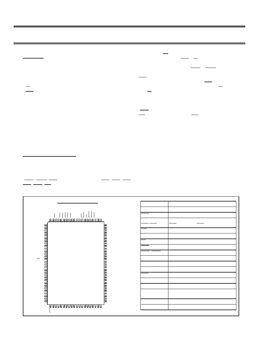
Pin configuration
Top view
100 pin QFP / TQFP
A
1
5
A0-15
Address Inputs
CLK
Clock Input
BWE
Byte Write Enable
BW1,BW2
BW3,BW4
Byte Write. BW1 for DQ1-8; BW2 for DQ9-16;
BW3 for DQ17-24; BW4 for DQ25-32
GW
Global Write Enable
CE1,CE2, CE3
Chip Enable
OE
Output Enable
ADV
Burst Address advance
ADSP, ADSC
Address Status
DQ1-32
Data I/O
ZZ
Power down control
FT
Flow-Thru mode
LBO
Linear Burst mode
VDD
3.3V Power Supply
VSS
Ground
VDDQ
Output
Power
Supply,
2.375V
to
VDD
(3.465Vmax)
VSSQ
Output Ground
NC
No Connect
Output enable (OE) and power down control (ZZ) are asynchro-
nous. 2 mode control pins (LBO & FT) define 4 operation modes
of linear/interleave burst order and output flow-thru/pipeline.
Burst can be initiated with either ADSP or ADSC inputs. Subse-
quent burst address are generated internally and are controlled by
ADV. The burst sequence is either interleave order (PentiumTM
and X86) or linear order and is defined by LBO.
Output registers are provided and are controlled by FT mode pin.
With FT mode pin, Output registers can be programmed in either
pipeline mode for very high frequency operation (117MHz) or
flow-thru mode for reduced latency.
Byte write operation can be obtained through byte write enable
(BWE) input combined with 4 individual byte write signals
BW1-4. In addition, global write (GW) signal is also available to
write all bytes at once.
Low power state (standby mode) can be obtained either through
the assertion of ZZ signal or simply stop the clock (CLK). In
standby mode, memory data are still retained. Low power design
of 0.5mA standby are provided on L version.
The GS820V32 operates from a 3.3V power supply and all
inputs and outputs are LVTTL compatible. Separate output
power (VDDQ) and ground (VSSQ) pins are employed to de-
couple output noise from internal circuit and VDDQ allow user
the flexibility to employ lower output supply level like 2.5V.
GS820V32’s interface level is also compatble to 2.5V supply
level.
The GS820V32 is implemented with GSI’s high performance
CMOS technology and is available in JEDEC standard 100 lead
QFP ( Q version ) and TQFP ( T version) package.
相关PDF资料 |
PDF描述 |
|---|---|
| GS8321E18AD-333IT | CACHE SRAM, PBGA165 |
| GS832236AB-150VT | 1M X 36 CACHE SRAM, 7.5 ns, PBGA119 |
| GS8342D11BD-500IT | 4M X 9 QDR SRAM, 0.45 ns, PBGA165 |
| GS8342D11BD-500 | 4M X 9 QDR SRAM, 0.45 ns, PBGA165 |
| GS8342D11BD-550IT | 4M X 9 QDR SRAM, 0.45 ns, PBGA165 |
相关代理商/技术参数 |
参数描述 |
|---|---|
| GS820V32Q | 制造商:GSI 制造商全称:GSI Technology 功能描述:64K x 32 Burst |
| GS820V32Q4 | 制造商:未知厂家 制造商全称:未知厂家 功能描述:x32 Fast Synchronous SRAM |
| GS820V32Q4I | 制造商:未知厂家 制造商全称:未知厂家 功能描述:x32 Fast Synchronous SRAM |
| GS820V32Q5 | 制造商:未知厂家 制造商全称:未知厂家 功能描述:x32 Fast Synchronous SRAM |
| GS820V32Q5I | 制造商:未知厂家 制造商全称:未知厂家 功能描述:x32 Fast Synchronous SRAM |
发布紧急采购,3分钟左右您将得到回复。