- 您现在的位置:买卖IC网 > PDF目录385341 > GS881Z18T-100I (GSI TECHNOLOGY) 8Mb Pipelined and Flow Through Synchronous NBT SRAMs PDF资料下载
参数资料
| 型号: | GS881Z18T-100I |
| 厂商: | GSI TECHNOLOGY |
| 元件分类: | DRAM |
| 英文描述: | 8Mb Pipelined and Flow Through Synchronous NBT SRAMs |
| 中文描述: | 512K X 18 ZBT SRAM, 12 ns, PQFP100 |
| 封装: | TQFP-100 |
| 文件页数: | 24/34页 |
| 文件大小: | 542K |
| 代理商: | GS881Z18T-100I |
第1页第2页第3页第4页第5页第6页第7页第8页第9页第10页第11页第12页第13页第14页第15页第16页第17页第18页第19页第20页第21页第22页第23页当前第24页第25页第26页第27页第28页第29页第30页第31页第32页第33页第34页
Rev: 1.10 8/2000
Specifications cited are subject to change without notice. For latest documentation see http://www.gsitechnology.com
24/34
1998, Giga Semconductor, Inc.
Preliminary
.
GS881Z18/36T-11/100/80/66
JTAG Port Operation
Overview
The JTAG Port on this RAM operates in a manner consistent with IEEE Standard 1149.1-1990, a serial boundary scan interface
standard (commonly referred to as JTAG), but does not implement all of the functions required for 1149.1 compliance. Some
functions have been modified or eliminated because they can slow the RAM. Nevertheless, the RAM supports 1149.1-1990 TAP
(Test Access Port) Controller architecture, and can be expected to function in a manner that does not conflict with the operation of
Standard 1149.1 compliant devices. The JTAG Port interfaces with conventional TTL / CMOS logic level signaling.
Disabling the JTAG Port
It is possible to use this device without utilizing the JTAG port. The port is reset at power-up and will remain inactive unless
clocked. TCK, TDI, and TMS are designed with internal pull-up circuits. To assure normal operation of the RAM with the JTAG
Port unused, TCK, TDI, and TMS may be left floating or tied to either V
DD
or V
SS
. TDO should be left unconnected.
JTAG Port Registers
Overview
The various JTAG registers, refered to as TAP Registers, are selected (one at a time) via the sequences of 1s and 0s applied to TMS
as TCK is strobed. Each of the TAP Registers are serial shift registers that capture serial input data on the rising edge of TCK and
push serial data out on the next falling edge of TCK. When a register is selected it is placed between the TDI and TDO pins.
Instruction Register
The Instruction Register holds the instructions that are executed by the TAP controller when it is moved into the Run, Test/Idle or
the various data register states. Instructions are 3 bits long. The Instruction Register can be loaded when it is placed between the
TDI and TDO pins. The Instruction Register is automatically preloaded with the IDCODE instruction at power-up or whenever the
controller is placed in Test-Logic-Reset state.
Bypass Register
The Bypass Register is a single-bit register that can be placed between TDI and TDO. It allows serial test data to be passed through
the RAMs JTAG Port to another device in the scan chain with as little delay as possible.
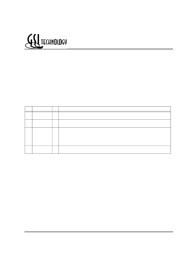
JTAG Pin Descriptions
Pin
Pin Name
I/O
Description
TCK
Test Clock
In
Clocks all TAP events. All inputs are captured on the rising edge of TCK and all outputs propagate fromthe
falling edge of TCK.
The TMS input is sampled on the rising edge of TCK. This is the command input for the TAP controller state
machine. An undriven TMS input will produce the same result as a logic one input level.
The TDI input is sampled on the rising edge of TCK. This is the input side of the serial registers placed
between TDI and TDO. The register placed between TDI and TDO is determned by the state of the TAP
Controller state machine and the instruction that is currently loaded in the TAP Instruction Register (refer to
the TAP Controller State Diagram. An undriven TDI pin will produce the same result as a logic one input
level.
Output that is active depending on the state of the TAP state machine. Output changes in response to the
falling edge of TCK. This is the output side of the serial registers placed between TDI and TDO.
TMS Test Mode Select
In
TDI
Test Data In
In
TDO
Test Data Out
Out
Note:
This device does not have a TRST (TAP Reset) pin. TRST is optional in IEEE 1149.1. The Test-Logic-Reset state is entered while TMS is
held high for five rising edges of TCK. The TAP Controller is also reset automaticly at power-up.
相关PDF资料 |
PDF描述 |
|---|---|
| GS881Z18T-11 | 8Mb Pipelined and Flow Through Synchronous NBT SRAMs |
| GS881Z18T-11I | 8Mb Pipelined and Flow Through Synchronous NBT SRAMs |
| GS881Z18T-66 | 8Mb Pipelined and Flow Through Synchronous NBT SRAMs |
| GS881Z18T-66I | 8Mb Pipelined and Flow Through Synchronous NBT SRAMs |
| GS881Z18T-80 | 8Mb Pipelined and Flow Through Synchronous NBT SRAMs |
相关代理商/技术参数 |
参数描述 |
|---|---|
| GS881Z18T-11 | 制造商:GSI 制造商全称:GSI Technology 功能描述:8Mb Pipelined and Flow Through Synchronous NBT SRAMs |
| GS881Z18T-11I | 制造商:GSI 制造商全称:GSI Technology 功能描述:8Mb Pipelined and Flow Through Synchronous NBT SRAMs |
| GS881Z18T-66 | 制造商:GSI 制造商全称:GSI Technology 功能描述:8Mb Pipelined and Flow Through Synchronous NBT SRAMs |
| GS881Z18T-66I | 制造商:GSI 制造商全称:GSI Technology 功能描述:8Mb Pipelined and Flow Through Synchronous NBT SRAMs |
| GS881Z18T-80 | 制造商:GSI 制造商全称:GSI Technology 功能描述:8Mb Pipelined and Flow Through Synchronous NBT SRAMs |
发布紧急采购,3分钟左右您将得到回复。