参数资料
| 型号: | HA3-5020-5Z |
| 厂商: | Intersil |
| 文件页数: | 2/23页 |
| 文件大小: | 0K |
| 描述: | IC AMP VIDEO CFA 100MHZ 8-DIP |
| 标准包装: | 50 |
| 应用: | 电流反馈 |
| 电路数: | 1 |
| -3db带宽: | 100MHz |
| 转换速率: | 1100 V/µs |
| 电流 - 电源: | 7.5mA |
| 电流 - 输出 / 通道: | 31.7mA |
| 电压 - 电源,单路/双路(±): | ±4.5 V ~ 18 V |
| 安装类型: | 通孔 |
| 封装/外壳: | 8-DIP(0.300",7.62mm) |
| 供应商设备封装: | 8-PDIP |
| 包装: | 管件 |
| 产品目录页面: | 1234 (CN2011-ZH PDF) |
10
FN2845.12
May 21, 2013
Application Information
Optimum Feedback Resistor
The plots of inverting and non-inverting frequency response
illustrate the performance of the HA-5020 in various closed
loop gain configurations. Although the bandwidth dependency
on closed loop gain isn’t as severe as that of a voltage
feedback amplifier, there can be an appreciable decrease in
bandwidth at higher gains. This decrease may be minimized
by taking advantage of the current feedback amplifier’s unique
relationship between bandwidth and RF. All current feedback
amplifiers require a feedback resistor, even for unity gain
applications, and RF, in conjunction with the internal
compensation capacitor, sets the dominant pole of the
frequency response. Thus, the amplifier’s bandwidth is
inversely proportional to RF. The HA-5020 design is optimized
for a 1000
Ω R
F at a gain of +1. Decreasing RF in a unity gain
application decreases stability, resulting in excessive peaking
and overshoot. At higher gains the amplifier is more stable, so
RF can be decreased in a trade-off of stability for bandwidth.
The table below lists recommended RF values for various
gains, and the expected bandwidth.
PC Board Layout
The frequency response of this amplifier depends greatly on
the amount of care taken in designing the PC board. The use
of low inductance components such as chip resistors and
chip capacitors is strongly recommended. If leaded
components are used the leads must be kept short
especially for the power supply decoupling components and
those components connected to the inverting input.
Attention must be given to decoupling the power supplies. A
large value (10F) tantalum or electrolytic capacitor in
parallel with a small value (0.1F) chip capacitor works well
in most cases.
A ground plane is strongly recommended to control noise. Care
must also be taken to minimize the capacitance to ground seen
by the amplifier’s inverting input (-IN). The larger this
capacitance, the worse the gain peaking, resulting in pulse
overshoot and possible instability. It is recommended that the
ground plane be removed under traces connected to -IN, and
that connections to -IN be kept as short as possible to minimize
the capacitance from this node to ground.
Driving Capacitive Loads
Capacitive loads will degrade the amplifier’s phase margin
resulting in frequency response peaking and possible
oscillations. In most cases the oscillation can be avoided by
placing an isolation resistor (R) in series with the output as
shown in Figure 6.
The selection criteria for the isolation resistor is highly
dependent on the load, but 27
Ω has been determined to be
a good starting value.
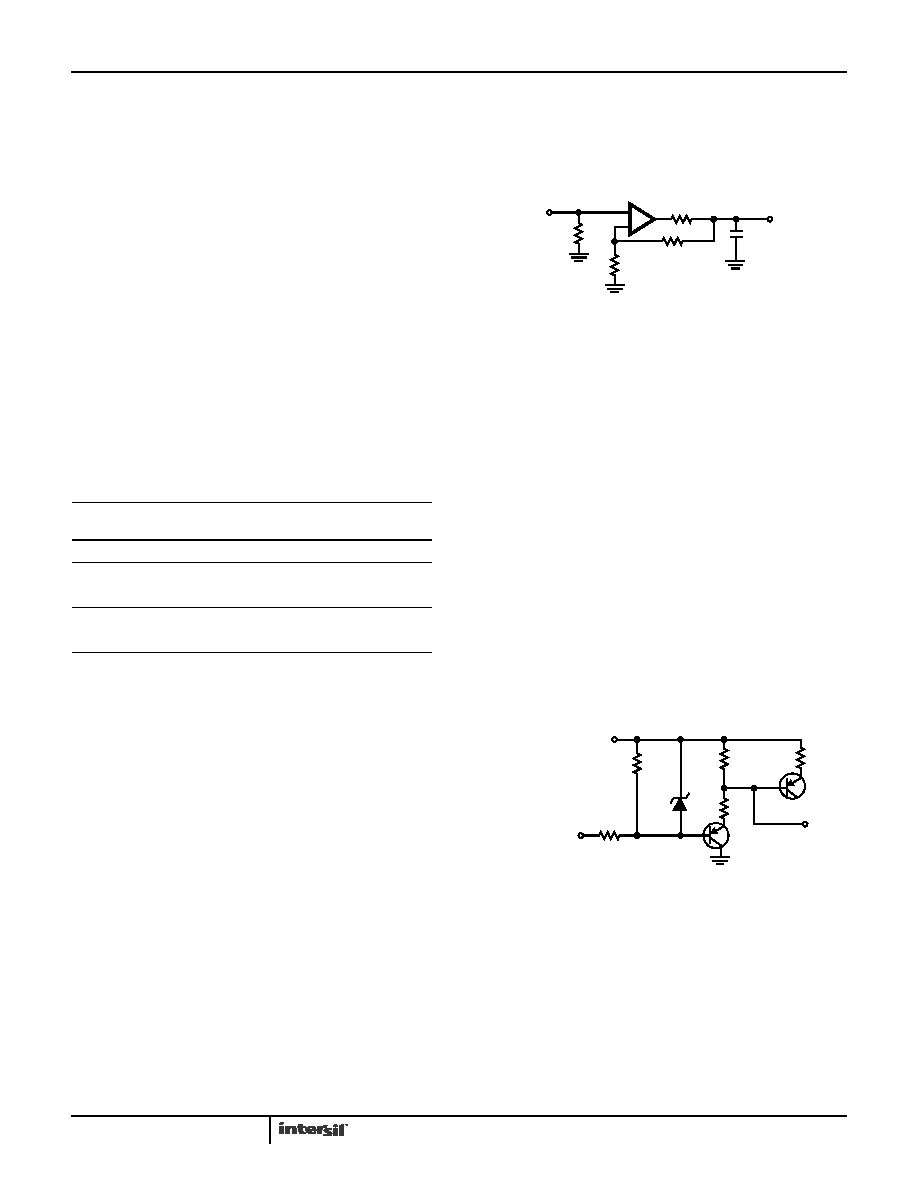
Enable/Disable Function
When enabled the amplifier functions as a normal current
feedback amplifier with all of the data in the electrical
specifications table being valid and applicable. When
disabled the amplifier output assumes a true high
impedance state and the supply current is reduced
significantly.
The circuit shown in Figure 7 is a simplified schematic of the
enable/disable function. The large value resistors in series
with the DISABLE pin makes it appear as a current source to
the driver. When the driver pulls this pin low current flows out
of the pin and into the driver. This current, which may be as
large as 350
μA when external circuit and process variables
are at their extremes, is required to insure that point “A”
achieves the proper potential to disable the output. The
driver must have the compliance and capability of sinking all
of this current.
When VCC is +5V the DISABLE pin may be driven with a
dedicated TTL gate. The maximum low level output voltage
of the TTL gate, 0.4V, has enough compliance to insure that
the amplifier will always be disabled even though D1 will not
turn on, and the TTL gate will sink enough current to keep
point “A” at its proper voltage. When VCC is greater than +5V
the DISABLE pin should be driven with an open collector
device that has a breakdown rating greater than VCC.
GAIN (ACL)RF (Ω)
BANDWIDTH
(MHz)
-1
750
100
+1
1000
125
+2
681
95
+5
1000
52
+10
383
65
-10
750
22
VIN
VOUT
CL
RT
+
-
RI
RF
R
FIGURE 6. PLACEMENT OF THE OUTPUT ISOLATION
RESISTOR, R
R6
15K
R7
15K
+VCC
ENABLE/
D1
QP3
R8
QP18
A
R33
R10
DISABLE INPUT
FIGURE 7. SIMPLIFIED SCHEMATIC OF ENABLE/DISABLE
FUNCTION
HA-5020
相关PDF资料 |
PDF描述 |
|---|---|
| HFA1105IBZ | IC OPAMP CFA 330MHZ LP 8-SOIC |
| VI-B1N-MU | CONVERTER MOD DC/DC 18.5V 200W |
| HA9P5020-5Z | IC AMP VIDEO 100MHZ CFB 8-SOIC |
| AD7226KN | IC DAC 8BIT LC2MOS QUAD 20-DIP |
| ISL59446IRZ-T7 | IC AMP MUX 4:1 500MHZ 32-QFN |
相关代理商/技术参数 |
参数描述 |
|---|---|
| HA3-5020-9 | 制造商:未知厂家 制造商全称:未知厂家 功能描述:Current-Feedback Operational Amplifier |
| HA3-5020R2548 | 制造商:Harris Corporation 功能描述: |
| HA350335 | 制造商:HAR 功能描述:350335 HAR'94 S10L2B 制造商:HARRIS 功能描述:IC S11L1C |
| HA3-5033-5 | 功能描述:IC VIDEO BUFFER 250MHZ 8-PDIP RoHS:否 类别:集成电路 (IC) >> 线性 - 放大器 - 视频放大器和频缓冲器 系列:- 标准包装:1,000 系列:- 应用:驱动器 输出类型:差分 电路数:3 -3db带宽:350MHz 转换速率:1000 V/µs 电流 - 电源:14.5mA 电流 - 输出 / 通道:60mA 电压 - 电源,单路/双路(±):5 V ~ 12 V,±2.5 V ~ 6 V 安装类型:表面贴装 封装/外壳:20-VFQFN 裸露焊盘 供应商设备封装:20-QFN 裸露焊盘(4x4) 包装:带卷 (TR) |
| HA350D | 制造商:Aleph America Corporation 功能描述: |
发布紧急采购,3分钟左右您将得到回复。