参数资料
| 型号: | HFA1110IBZ |
| 厂商: | Intersil |
| 文件页数: | 3/9页 |
| 文件大小: | 0K |
| 描述: | IC BUFFER C-LOOP 750MHZ LD 8SOIC |
| 标准包装: | 98 |
| 放大器类型: | 缓冲器 |
| 电路数: | 1 |
| 转换速率: | 1300 V/µs |
| -3db带宽: | 750MHz |
| 电流 - 输入偏压: | 10µA |
| 电压 - 输入偏移: | 8000µV |
| 电流 - 电源: | 21mA |
| 电流 - 输出 / 通道: | 60mA |
| 电压 - 电源,单路/双路(±): | 9 V ~ 11 V,±4.5 V ~ 5.5 V |
| 工作温度: | -40°C ~ 85°C |
| 安装类型: | 表面贴装 |
| 封装/外壳: | 8-SOIC(0.154",3.90mm 宽) |
| 供应商设备封装: | 8-SOIC |
| 包装: | 管件 |
| 产品目录页面: | 1234 (CN2011-ZH PDF) |
3
FN2944.8
June 6, 2006
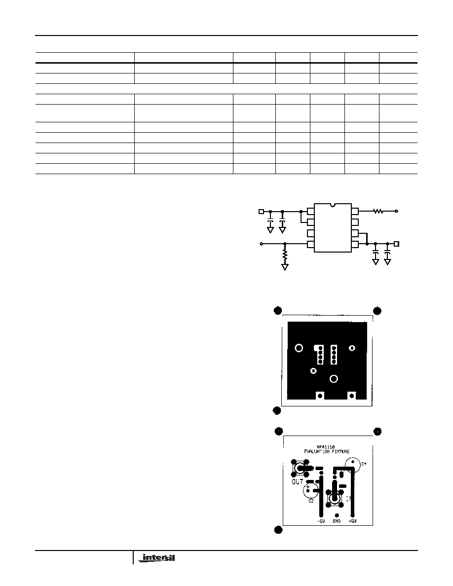
Application Information
PC Board Layout
The frequency performance of this amplifier depends a great
deal on the amount of care taken in designing the PC board.
The use of low inductance components such as chip
resistors and chip capacitors is strongly recommended,
while a solid ground plane is a must!
Attention should be given to decoupling the power supplies.
A large value (10
F) tantalum in parallel with a small value
chip (0.1
F) capacitor works well in most cases.
Terminated microstrip signal lines are recommended at the
input and output of the device. Output capacitance, such as
that resulting from an improperly terminated transmission
line will degrade the frequency response of the amplifier and
may cause oscillations. In most cases, the oscillation can be
avoided by placing a resistor (RS) in series with the output.
See the “Recommended RS vs Load Capacitance” graph for
specific recommendations.
An example of a good high frequency layout is the
Evaluation Board shown below.
Evaluation Board
An evaluation board is available for the HFA1110 (part
number HFA1110EVAL). Please contact your local sales
office for information.
The layout and schematic of the board are shown here:
NOTE: The SOIC version may be evaluated in the DIP board by
using a SOIC-to-DIP adapter such as Aries Electronics Part Number
08-350000-10.
-1dB Gain Compression
100MHz
25
-
14
-
dBm
Reverse Gain (S12, Note 2)
100MHz, VOUT = 1VP-P
25
-
-60
-
dB
TRANSIENT RESPONSE
Rise Time
VOUT = 0.5V Step
25
-
0.5
-
ns
Overshoot (Note 2)
VOUT = 1.0V Step, Input Signal
Rise/Fall = 1ns
25
-
2.5
-
%
0.2% Settling Time (Note 2)
VOUT = 1V to 0V
25
-
7
-
ns
0.1% Settling Time (Note 2)
VOUT = 1V to 0V
25
-
11
-
ns
Overdrive Recovery Time
25
-
15
-
ns
Differential Gain
3.58MHz, RL = 75
25
-
0.04
-
%
Differential Phase
3.58MHz, RL = 75
25
-
0.025
-
°
NOTE:
2. See Typical Performance Curves for more information.
Electrical Specifications
VSUPPLY = ±5V, RL = 100, Unless Otherwise Specified (Continued)
PARAMETER
TEST CONDITIONS
TEMP (°C)
MIN
TYP
MAX
UNITS
50
1
2
3
4
8
7
6
5
+5V
0.1
F10F
50
OUT
0.1
F
10
F
-5V
HFA1110
IN
RS
SCHEMATIC DIAGRAM
BOTTOM LAYOUT
TOP LAYOUT
1
HFA1110
相关PDF资料 |
PDF描述 |
|---|---|
| HFA1112IPZ | IC AMP BUFFER 850MHZ LD 8-PDIP |
| HFA1113IBZ | IC BUFFER 850MHZ 8-SOIC |
| HFA1130IBZ | IC OP AMP 850MHZ CFB 8-SOIC |
| HFA1412IP | IC BUFFER QUAD 350MHZ LP 14-DIP |
| HS18 | HEATSINK 12P PDIP |
相关代理商/技术参数 |
参数描述 |
|---|---|
| HFA1110IJ | 制造商:Harris Corporation 功能描述: |
| HFA1110IP | 制造商:Rochester Electronics LLC 功能描述:850MHZ UNITY GAIN BUFFER,8 PIN PDIP - Bulk |
| HFA1110MJ/883 | 制造商:Rochester Electronics LLC 功能描述:- Bulk |
| HFA1112 | 制造商:INTERSIL 制造商全称:Intersil Corporation 功能描述:850MHz, Low Distortion Programmable Gain Buffer Amplifier |
| HFA1112 WAF | 制造商:Intersil Corporation 功能描述: |
发布紧急采购,3分钟左右您将得到回复。