- 您现在的位置:买卖IC网 > PDF目录385375 > HFA1115 (Intersil Corporation) 225MHz, Low Power, Output Limiting, Closed Loop Buffer Amplifier(225MHz、低功耗、输出限定锁相环缓冲器放大器) PDF资料下载
参数资料
| 型号: | HFA1115 |
| 厂商: | Intersil Corporation |
| 英文描述: | 225MHz, Low Power, Output Limiting, Closed Loop Buffer Amplifier(225MHz、低功耗、输出限定锁相环缓冲器放大器) |
| 中文描述: | 225MHz?1800MHz的,低功耗,输出限制,闭环缓冲放大器(225MHz?1800MHz的,低功耗,输出限定锁相环缓冲器放大器) |
| 文件页数: | 7/14页 |
| 文件大小: | 159K |
| 代理商: | HFA1115 |
7
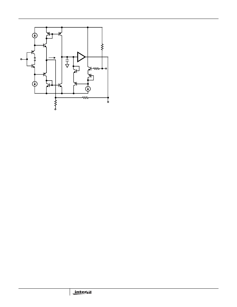
This current is mirrored onto the high impedance node (Z) by
Q
X3
-Q
X4
, where it is converted to a voltage and fed to the
output via another unity gain buffer. If no limiting is utilized,
the high impedance node may swing within the limits defined
by Q
P4
and Q
N4
. Note that when the output reaches its
quiescent value, the current flowing through -IN is reduced to
only that small current (-I
BIAS
) required to keep the output at
the final voltage.
Tracing the path from V
H
to Z illustrates the effect of the limit
voltage on the high impedance node. V
H
decreases by 2V
BE
(Q
N6
and Q
P6
) to set up the base voltage on Q
P5
. Q
P5
begins to conduct whenever the high impedance node
reaches a voltage equal to Q
P5
’s base voltage + 2V
BE
(Q
P5
and Q
N5
). Thus, Q
P5
limits node Z whenever Z reaches V
H
.
R
1
provides a pull-up network to ensure functionality with the
limit inputs floating. A similar description applies to the
symmetrical low limit circuitry controlled by V
L
.
When the output is limited, the negative input continues to
source a slewing current (I
Limit
) in an attempt to force the
output to the quiescent voltage defined by the input. Q
P5
must sink this current while limiting, because the -IN current
is always mirrored onto the high impedance node. The
limiting current is calculated as:
I
LIMIT
= (V
-IN
- V
OUT LIMITED
)/R
F
+ V
-IN
/R
G
.
As an example, a unity gain circuit with V
IN
= 2V, and V
H
= 1V,
would have I
LIMIT
= (2V - 1V)/350
+ 2V/
∞
= 2.8mA (R
G
=
∞
because -IN is floated for unity gain applications). Note that I
CC
increases by I
LIMIT
when the output is limited.
Limit Accuracy
The limited output voltage will not be exactly equal to the
voltage applied to V
H
or V
L
. Offset errors, mostly due to V
BE
mismatches, necessitate a limit accuracy parameter which is
found in the device specifications. Limit accuracy is a
function of the limiting conditions. Referring again to Figure
3, it can be seen that one component of limit accuracy is the
V
BE
mismatch between the Q
X6
transistors, and the Q
X5
transistors. If the transistors always ran at the same current
level there would be no V
BE
mismatch, and no contribution
to the inaccuracy. The Q
X6
transistors are biased at a
constant current, but as described earlier, the current
through Q
X5
is equivalent to I
Limit
. V
BE
increases as I
LIMIT
increases, causing the limited output voltage to increase as
well. I
LIMIT
is a function of the overdrive level
((A
V
x V
IN
- V
LIMIT
) / V
LIMIT
), so limit accuracy degrades as
the overdrive increases (see Figures 28 and 29). For
example, accuracy degrades from -20mV to +30mV when
the overdrive increases from 100% to 200% (A
V
= +2,
V
H
= 500mV
).
Consideration must also be given to the fact that the limit
voltages have an effect on amplifier linearity. The “Linearity
Near Limit Voltage” curves, Figures 30 and 31, illustrate the
impact of several limit levels on linearity.
Limit Range
Unlike some competitor devices, both V
H
and V
L
have
usable ranges that cross 0V. While V
H
must be more
positive than V
L
, both may be positive or negative, within
the range restrictions indicated in the specifications. For
example, the HFA1115 could be limited to ECL output
levels by setting V
H
= -0.8V and V
L
= -1.8V. V
H
and V
L
may
be connected to the same voltage (GND for instance) but
the result won’t be a DC output voltage from an AC input
signal. A 150mV - 200mV AC signal will still be present at
the output.
Recovery from Overdrive
The output voltage remains at the limit level as long as the
overdrive condition remains. When the input voltage drops
below the overdrive level (V
LIMIT
/A
V
) the amplifier returns to
linear operation. A time delay, known as the Overdrive
Recovery Time, is required for this resumption of linear
operation. Overdrive recovery time is defined as the
difference between the amplifier’s propagation delay exiting
limiting and the amplifier’s normal propagation delay, and it is
a strong function of the overdrive level. Figure 32 details the
overdrive recovery time for various limit and overdrive levels
Benefits of Output Limiting
The plots of “Pulse Response Without Limiting” and “Pulse
Response With Limiting” (Figures 4 and 5) highlight the
advantages of output limiting. Besides the obvious benefit of
constraining the output swing to a defined range, limiting the
output excursions also keeps the output transistors from
saturating, which prevents unwanted saturation artifacts
from distorting the output signal. Output limiting also takes
advantage of the HFA1115’s ultra-fast overdrive recovery
time, reducing the recovery time from 2.5ns to 0.5ns, based
on the amplifier’s normal propagation delay of 1.2ns.
+1
+IN
V-
V+
Q
P1
Q
N1
V-
Q
N3
Q
P3
Q
P4
Q
N2
Q
P2
Q
N4
Q
P5
Q
N5
Z
V+
-IN
V
OUT
I
LIMIT
Q
P6
Q
N6
V
H
R
1
V
-IN
200
FIGURE 3. HFA1115 SIMPLIFIED V
H
LIMIT CIRCUITRY
50k
R
F
= 350
(INTERNAL)
R
G
= 350
(INTERNAL)
HFA1115
相关PDF资料 |
PDF描述 |
|---|---|
| HFA1130 | 850MHz, Output Limiting, Low Distortion Current Feedback Operational Amplifier(850MHz、输出额定、低失真电流反馈运算放大器) |
| HFA1135IB96 | GT 3C 3#16S SKT RECP BOX |
| HFA1135IB | 360MHz, Low Power, Video Operational Amplifier with Output Limiting |
| HFA1135EVAL | 360MHz, Low Power, Video Operational Amplifier with Output Limiting |
| HFA1135 | 360MHz, Low Power, Video Operational Amplifier with Output Limiting(360MHz、低功耗视频运算放大器(带输出限制)) |
相关代理商/技术参数 |
参数描述 |
|---|---|
| HFA1115/883 | 制造商:INTERSIL 制造商全称:Intersil Corporation 功能描述:High Speed, Low Power, Output Limiting Closed Loop Buffer Amplifier |
| HFA1115_04 | 制造商:INTERSIL 制造商全称:Intersil Corporation 功能描述:225MHz, Low Power, Output Limiting, Closed Loop Buffer Amplifier |
| HFA1115883 | 制造商:INTERSIL 制造商全称:Intersil Corporation 功能描述:High Speed, Low Power, Output Limiting Closed Loop Buffer Amplifier |
| HFA1115EVAL | 制造商:INTERSIL 制造商全称:Intersil Corporation 功能描述:225MHz, Low Power, Output Limiting, Closed Loop Buffer Amplifier |
| HFA1115IB | 制造商:Rochester Electronics LLC 功能描述:BUFFER 225MHZ CFB PRG-GAIN CLMP 8SOIC IND - Bulk |
发布紧急采购,3分钟左右您将得到回复。